Friday, October 31, 2014

Digital Isolation up to 100 Mbits Diagram Circuit

When it is necessary to send a digital signal between two electrically isolated circuits you would normally choose an optoisolator or some form of transformer coupling. Neither of these solutions is ideal; optocouplers run out of steam beyond about 10 MHz and transformers do not have a good low frequency (in the region of Hertz) response. The company NVE Corporation (www.nve.com) produces a range of coupler devices using an innovative ‘IsoLoop’ technology allowing data rates up to 110 Mbaud. The example shown here uses the IL715 type coupler providing four TTL or CMOS compatible channels with a data rate of 100 Mbit/s. Inputs and outputs are compatible with 3.3 V or 5 V systems. The maximum isolation voltage is 2.5 kV and the device can cope with input transients up to 20 kV/µs.

Circuit diagram:

The company produce many other configurations including bidirectional versions that would be suitable for RS485 interfacing. The IsoLoop coupler is based on relatively new GMR (GiantMagnetoResistive) technology. The input signal produces a current in a planar coil. This current generates a magnetic field that produces a change in resistance of the GMR material. This material is isolated from the planar coil by a thin film high voltage insulating layer. The change in resistance is amplified and fed to a comparator to produce a digital output signal. Differences in the ground potential of either the input or output stage will not produce any current flow in the planar coil and therefore no magnetic field changes to affect the GMR material. Altogether the circuit provides a good electrical isolation between input and output and also protects against input signal transients (EMV).
Author: Gregor Kleine - Copyright: Elektor July-August 200
Read More..

LM317 to create constant current of 2mA

I have a circuit where I want to have a constant current of 2mA through a variable resistor. Ive been told that I could probably use a LM317 as a current regulator, with one resistor on the ouput. But Ive read some places that the LM317 takes minimum 5-10mA load to function correctly.

How can I achieve a constant current output of 2mA when I dont know the resistance of the variable resistor?

The input voltage is about 2.755V. Output voltage doesnt matter, just the current.


Heres an image to my feeble attempt at a schematic:


enter


The LM317 with the single series resistor between output and adjust input is actually a fixed current source, not a current limiter. You dont need the LM317 to create a current limiter, a few discrete components will do:
enter
For a limiting at 2mA you select a 330Ω resistor for RSENSE. If there flows 2mA through it Q2 will start to conduct and reduce the base voltage of Q1, so that its current is cut off.
edit (re changed question)

Maybe youre focusing too much on the LM317. If you need a constant current you could use the LM234 which is a programmable current source for up to 10mA. You set the current with a resistor.
Read More..

24V DC Powered Beeper with 4 Separate Inputs

24 Volt DC is a very prevalent voltage used fashionable developed settings. This hobby circuit lower was designed to acknowledge four unlike 24v DC alarm input signals, which are followed by used to drive a single low power beeper. The beeper is a magnetic type with its own oscillator/driver. The four diodes form an “or else” gate so one solitary of the four inputs want cause the beeper to produce blast. A CMOS version of the widely held 555 timer is used to strobe the beeper on and rancid on something like 1Hz.

24V DC Powered Beeper with 4 Separate Inputs Circuit Schematic Diagram

Read More..

Isolated Fuse Fail Indicator Circuit Diagram

This is the simple Isolated Fuse Fail Indicator Circuit Diagram. This circuit uses standard components and shows a method of indicating the fuse status of mains powered equipment while providing electrical isolation from the mains supply.


Isolated Fuse Fail Indicator Circuit diagram:

Isolated
Isolated Fuse Fail Indicator Circuit Diagram

A standard miniature low power mains transformer  (e.g. with an output of around 6 V at 1.5 VA) is used as a ‘sense’ trans-former with its primary winding (230 V) connected across the equipment’s input fuse so that when the fuse blows, mains voltage is applied to the transformer and a 6 V ac output volt-age appears at the secondary winding. The 1N4148 diode rectifies this voltage and the LED lights to indicate that the fuse has failed. The rectified voltage is now connected to an RC low-pass filter formed by the 10 kΩ resistor and 100 nF capacitor. The resulting positive signal can now be used as an input to an A/D converter or as a digital input to a microcontroller (make sure that the signal level is within the microcontroller input voltage level specification). The 1 MΩ resistor is used to discharge the capacitor if the input impedance of the connected equipment is very high.

As long as the fuse remains intact it will short out the primary winding of the ‘sense’ transformer so that its secondary out-put is zero.
Read More..

Thursday, October 30, 2014

Mp3 Booster Pump it up Diagram Circuit

MP3 players are all the rage these days. The smaller ones in memory-stick format are particularly easy to take with you; your very own ‘personal sound system’ on the move! It’s when you want others to share your taste in music that you find these players to have a lack of power. You can get round this problem with the help of the MP3 booster, a small amplifier that can be used to connect your MP3 player directly to your Hi-Fi. When you next invite your friends to a party you can ask them to bring their ‘personal music’ as well as the usual drinks!

But first we have to build this booster! The small battery-powered players have an output signal that is more than sufficient to drive a set of 32 Ohm headphones. You’ll often find that with an output of 1mW the sound pressure level (SPL) produced can reach up to 90 dB. This would be sufficient to cause permanent damage to your hearing after only one hour! The maximum output voltage will then be around 200mV. This, however, is insufficient to fully drive a power amplifier. For this you’ll need an extra circuit that boosts the output voltage.

Power amps usually require 1 V for maximum output, hence the signal has to be amplified by a factor of five. We will also have to bear in mind that quieter recordings may need to be amplified even more. We’ve used a simple method here to select the gain, which avoids the use of potentiometers. After all, the MP3 player already has its own volume control. We decided to have two gain settings on the booster, one of three times and the other ten times. Amplifiers IC1A and IC1B (for the right and left channels) are housed in a single package, a TS922IN.

The output signal of the MP3 player is fed via a stereo cable and socket K1 to the inputs of the amplifiers. The gain depends on the relationship between resistors R2 and R1 (R6 and R5 for the other channel) and is equal to ten times. When you add jumper JP1 (JP2), resistor R3 (R7) will be connected in parallel with the negative feedback resistor R1 (R6), which causes the gain to be reduced to about three. When you start using the booster you can decide which gain setting works best for you.

Circuit diagram:
MP3 Booster Circuit Diagram

Resistor R4 (R8) takes the amplified MP3 signal to the output socket K2 (K3). A cable then connects these phono sockets to the input of your power amplifier. The resistors connected in series with the output (R4 and R8) are there to keep the booster stable when a long cable is connected to its output. Cables have an unwelcome, parasitic capacitance. This capacitive effect could (due to phase shifts of the signal) affect the negative feedback of the booster in such a way that a positive feed back occurs, with the result that the booster oscillates and possibly damages the power amplifier!

The resistors (R4 and R8) effectively isolate the output of the booster from the parasitic capacitance of the output cable. They also protect the booster outputs from short circuits. We’ve used a TS922IN opamp in this booster because it can operate at very low supply voltages (the maximum is only 12 V!), but can still output a reasonable current (80 mA max.). For the supply we’ve used rechargeable batteries (e.g. NiCd or NiMH cells) so that we don’t need a mains supply.

To keep the number of cells required as small as possible, we’ve chosen a supply voltage of 5 volt; this can be supplied by four rechargeable batteries. It is also possible to use four ordinary, non-rechargeable batteries; it’s true that the supply voltage then becomes a bit higher (6 Volts), but that won’t cause any harm. Since we’ve used a symmetrical supply for the booster (2 x 2 batteries), it will be easiest if you use two separate battery holders, each with two AA cells. The two holders are connected in series.

Make sure that the batteries are connected the right way round; the positive of one always has to be connected to the negative of the next. This also applies to the connection between the two battery holders. S1A/B is a double pole switch, which is used to turn both halves of the battery supply on or off simultaneously. If you can’t find the (dual) opamp we’ve used (or an equivalent), you could always use standard opamps such as the NE5532, TL082 or TL072. These do need a higher supply voltage to operate properly. In these cases you should use two 9 V batteries and replace resistor R9 with a 15 kΩ one.

Do take care when you connect the circuit to your power amplifier because the output signal can be a lot larger and you could overload the power amplifier. (Although you’re more likely to damage the loudspeakers, rather than the amplifier!) (Please note that these two 9 V batteries can’t be used as a supply for the TS922IN!) In our circuit we’ve used a stereo jack socket for the input and phono sockets for the output because these are the most compatible with MP3 players and power amplifiers respectively. If you wanted to, you could solder shielded cables directly to the circuit instead, with the correct plugs on the ends. You’ll never find yourself without the correct connection leads in that case! 
Read More..

TDA2003 Car audio amplifier Diagram Circuit


Car Audio Amplifier Circuit

Description.

A simple low power car stereo amplifier circuit based on TDA 2003 is shown here. The circuit uses cheap, readily available components and it is very easy to construct. TDA2003 is an integrated car radio amplifier from ST Micro electronics that has a lot of good features like short circuit protection for all pins, thermal over range low harmonic distortion, low cross over distortion etc.
In the circuit given here each TDA2003 is wired as a mono amplifier operating from a 12V supply. Resistors R2 and R3 forms a feedback network that sets the amplifiers gain. C7 is the input DC de-coupling capacitor and C5 couples the speaker to the amplifiers output. C4 is used for improving the ripple rejection while C1 and C2 are employed for power supply filtering. C3 and R1 are used for setting the upper frequency cut-off. Network comprising of C6 and R4 is used for frequency stabilization and to prevent oscillation.

Car audio amplifier Circuit diagram.


Car stereo amplifier circuit schematic

Notes.

  • Assemble the circuit on a good quality PCB.
  • Heat sinks are necessary for both ICs.
  • The circuit can be operated from 12V DC.
  • S1 is the ON/OFF switch.
Read More..

LED Flashlight Use Supercapacitor


Bored of playing around with capacitors? Then its time for you to move on to super-capacitors. These have huge storage capabilities. In this article you will find out how to build a small LED flashlight using supercapacitors.

LED

The main disadvantage of capacitors is their large voltage drop. For this project, a minimum voltage of 2 volts is required to light the LED. As a result, the “Joule Thief” design would be incorporated here. Using this, a AA battery can be used to light an LED till it is completely discharged.
In this case, a supercapacitor would be taking the place of the battery. Here an LED is used to perform the function of a diode. This ensures that there is sufficient voltage across the LED.

LED

The requirements of the project are listed below:
  • White LED
  • Super capacitor (10F, 2.7 V)
  • Transistor
  • Torus
  • 1 k ohm resistor
  • Wires
  • Breadboard

The torus and the transistor used here comes from an energy-saving lamp HS. Care should be taken while removing this from the lamp as a breakage could result in the release of the mercury vapors. A lamp load along with a USB port is added to the circuit. This makes it compatible with a PC or a car radio.

LED

 A few precautions have to be taken while constructing the circuit. The USB port should not be provided with excess power. The capacitor does not withstand a high voltage and hence a zener diode is connected in parallel to handle the high voltage. The diode protects the capacitor when the voltage exceeds a certain value.
Read More..

USB Keyboard Made from Old Typewriter

Looking for a unique gift? Here’s an antique typewriter which has been modified to function as a USB Keyboard for PC, Mac, or even iPad. That’s very cool, isn’t it?


In the world of obsolescence, this USB typewriter is a groundbreaking innovation. It does not change the outward appearance of the typewriter and is easy to install since there is no messy wiring. The 3 components of the USB typewriter are the Sensor board, the USB switches, and the Reed Switches.

It works like a regular typewriter with all letters, numerals, and punctuation marks as well as shift, space, and return carriage. It’s a better addition to your home office.
Read More..

Stereo Amplifier for Laptop


Miniature Stereo amplifier,low power, a lesser amount of procedure, IC TDA7025 is the major equipment. undertaking of the circuit, the sign split into absent and well through the capacitor coupling of C1, C2 is a adaptable resistor VR1 adjusts the strength of the input signals to connection amplifiers power suppliers IC1-. IC2, serves to amplify the indicate up, drive not worth it the speakers absent - right.

Stereo
Stereo Amplifier for Laptoo Schematic Circuit
Resistors R1, R2 regulate the input impedance to the circuit box,The capacitor C4, the current filter to smooth and C1 reduce racket, and penetrating frequency, follow-on from the power supply to ground. It helps to stabilize the circuit.

Circuit power supply: 6-volt battery or else batteries, just 4 watts of output power up to 1.5 watts by the side of 8-ohm speakers to the sound of insignificant box, data lines, videotape player. It’s a light or else sound. refusal lone was banned. individual has a headset jack or else the phone becomes offered.
Read More..

Wednesday, October 29, 2014

5 18V Stabilized Power Supply This power supply will give you fixed regulated output at 5V 6V 9V and 12V while the 18V output is unregulated You c

5-18V Stabilized Power Supply

This power supply will give you fixed regulated output at 5V, 6V, 9V and 12V, while the 18V output is unregulated. You could add some regulated IC like LM7815 or 7818 if you need higher output voltage.
electronic


This circuit provide an audio indicator that will act like an alarm if any circuit short contact.
Read More..

Error Correction Output Stage for Mosfet and BJT Power Amplifier

For best results, any active device with the exception of the output transistors operating in class A. This is to avoid bias to saturate or block the entrance to all the clipping level, should be selected. This raises some difficulties for a BJT amplifier, where (to stay in Class A) driver stage collector currents, the base of BJT output current at maximum output current (ie in our case some of 10A) No is not exceeded. Therefore, the overall bias regime redesigned to allow space for the swing base BJT output current.

Error

Even in these circumstances, the power dissipation in the driver’s relevant and it is doubtful if a heat sink on board (as in our design side MOSFET included) help, if maximum performance is desired 200W into 4 ohms. It is therefore assumed that the power BJT design based on our application can not be more than one goal and 100W/4ohm 50W/8ohm. Of course, for such relatively modest achievements, it is not necessary to install three pairs of output devices, a pair of (ex) MJL4281/MJL4302 or equivalent work will be done.

Adjusting the balance Hawks Word is a double potentiometer (minimum of ten rounds) with more than 0.5% of correspondence between the sections. We replaced R20 and R81 with a 2K potentiometer Bourns 10 turns and adjusted for minimum distortion 20kHz Open Loop. You will find that the minimum is strongly dependent on the frequency, always adapting to at least the higher frequency in the audible range. At low frequencies, the feedback loop gain in reducing DHT levels to help you. Measured values ??and replace the potentiometer with fixed resistors.

The minimum is usually very close, if you need 0.5% or better precision resistors. The aim should be to bring the open-loop THD-20 below 0.01% to 10 Vrms input level. We built four previous CE FPO advice and got the last open-loop THD-20-values ??at 0.0065% 0.0075% 0.0090% and 0.012% (the latter, we can not source of precision resistors required values).

The network output Zobel is the stability amps together. For the same reasons, shoud not be 2UH air core output inductor.

The error amplifier frequency compensation C17 is the signal ground of the amplifier that takes full power to the ground. It is for reasons of stability and provide a grounding shield for feedback (output port).
Read More..

LM331 Frequency to voltage converter Diagram Circuit

Description.
LM331 is basically a precision voltage to frequency converter from National Semiconductors. The IC has a hand full of applications like analog to digital conversion, long term integration, voltage to frequency conversion, frequency to voltage conversion. Wide dynamic range and excellent linearity makes the IC well suitable for the applications mentioned above.
Here the LM331 is wired as a frequency to voltage converter which converts the input frequency into a proportional voltage which is extremely linear to the input frequency. The frequency to voltage conversion is attained by differentiating the input frequency using capacitor C3 and resistor R7 and feeding the resultant pulse train to the pin6 (threshold) of the IC. The negative going edge of the resultant pulse train at pin6 makes the built-in comparator circuit to trigger the timer circuit. At any instant, the current flowing out of the current output pin (pin 6) will be proportional to the input frequency and value of the timing components (R1 and C1). As a result a voltage (Vout) proportional to the input frequency (Fin) will be available across the load resistor R4.
Circuit diagram.
Notes.
  • The circuit can be assembled on a vero board.
  • I used 15V DC as the supply voltage (+Vs) while testing the circuit.
  • The LM331 can be operated from anything between 5 to 30V DC.
  • The value of R3 depends on the supply voltage and the equation is R3= (Vs – 2V)/ (2mA).
  • According to the equation, for Vs = 15V, R3=68K.
  • The output voltage depends on the equation, Vout = ((R4)/(R5+R6))*R1C1*2.09V*Fin.
  • POT R6 can be used for calibrating the circuit.
Read More..

Beat frequency Oscillator Simple Metal Detector Schematic

Beat-frequencyThis simple metal detector requires alone a scattering of apparatus and an evening’s work. Congenital about a cmos4011 IC, is actual able-bodied and versatile. The 250 kHz advertence oscillator is congenital with two gates (U1/1 and U1/2), C1, R1 and P1. The chase oscillator uses alone one aboideau (U1/3), two capacitors and the chase coil. The outputs of the two oscillators are fed to the fourth aboideau acting as a mixer and filtered with C4.

After assembly, affix the headphones and boring about-face P1. The angle will get lower until it disappears. Continuing to circle P1 in the aforementioned administration will account the angle to acceleration again. The point at witch the angle is the everyman and disappears is alleged “zero beat”. If you can not get this aught exhausted abundance for the absolute about-face of P1 you may accept to baddest altered ethics for C1.

Turn P1 abutting to the aught exhausted position, again move the chase braid abreast a brownish object. The accent should change, depending on the admeasurement and ambit of the metal.

Note that this simple detector’s achievement is not commensurable to added avant-garde bartering products. It will alone ascertain about ample brownish altar at a abbreviate distance. Coins and added baby altar will be abundant harder to find!

Here the Beat-frequency Oscillator Simple Metal Detector Schematic Part List :

  • U1: CD4011 (Quad 2-input NAND Gate)
  • U2: LM78L05 (5V Regulator IC)
  • R1: 2.2k 5% resistor
  • R3: 330k 5% resistor
  • R4: 270k 5% resistor
  • R5: 1k 5% resistor
  • C1: 390pF NPO capacitor
  • C2, C3: 10nF
  • C4: 100nF
  • C5: 100uF/16V electrolytic
  • C6: 220uF/16V electrolytic
  • C7: 100nF ceramic
  • P1: 4.7k lin. potentiometer
  • L1: 22cm diameter, 14 turns, AWG 26
  • K1: SPDT toggle switch
  • J1: Headphone jack 1/4 or 1/8 inch
Read More..

Proximity Detector Circuit Diagram

This is the simple Proximity Detector Circuit Diagram. This proximity detector is constructed using an infrared diode detector. Infrared detector can be used in various equipment such as burglar alarms, touch free proximity switches for turning on a light, and solenoid-controlled valves for operating a water tap. Briefly, the circuit consists of an infrared transmitter and an infra-red receiver (such as Siemens SFH506-38 used in TV sets).

  The transmitter part consists of two 555 timers (IC1 and IC2) wired in astable mode, as shown in the figure, for driving an infrared LED. A burst output of 38 kHz, modulated at 100 Hz, is required for the infrared detector to sense the trans mission; hence the setup as shown is required.  To save power, the duty cycle of the 38kHz astable multivibrator is maintained at 10 per cent.  The receiver part has an infrared detector comprising IC 555 (IC3), wired for operation in monostable mode, followed by pnp transistor T1. Upon reception of infrared signals, the 555 timer (mono) is turned  ‘on’ and it re-mains  ‘on’ as long as the infrared signals are being received.

Proximity Detector Circuit Diagram:
 
Proximity
Proximity Detector Circuit Diagram
 
When no more signals are received, the mono goes  ‘off’ after a few seconds (the delay depends on timing resistor-capacitor combination of R7-C5). The de-lay obtained using 470kilo-ohm resistor and 4.7µF capacitor is about 3 seconds. Unlike an ordinary mono, the capacitor in this mono is allowed to charge only when the reception of the signal has stopped, because of the pnp transistor T1 that shorts the charging capacitor as long as the output from IR receiver module is available (active low).  This setup can be used to detect proximity of an object moving by. Both transmitter and receiver can be mounted on a single breadboard/PCB, but care should be taken that infrared receiver is behind the infrared LED, so that the problem due to infrared leak-age is obviated.  

An object moving nearby actually reflects the infrared rays from the infrared LED. As the infrared receiver has a sensitivity angle of 60o, the IR rays are sensed within this lobe and the mono in the receiver section is triggered. This principle can be used to turn ‘on’ the light, using a relay, when a person comes nearby. The same automatically turns  ‘off’ after some time, as the person moves away. The sensitivity depends on the current limiting resistor in series with the infrared LED. It is ob-served that with in circuit resistance of preset VR1 set at 20 ohms, the object at a distance of about 25 cms can be sensed.  This circuit can be used for burglar alarms based on beam interruption, with the added advantage that the transmitter and receiver are housed in the same enclosure, avoiding any wiring problems.
Read More..

Temperature Candle Using LED

LED based projects require a lot of skill and hence only experienced circuit designers try out these circuits. But there are also a few circuits in this genre that can be done by amateur electronic hobbyists. The temperature candle is one such circuit. Read on to know more about this.


The hardware components that are required to build this circuit are listed below:
  • Microcontroller
  • Temperature Sensor
  • RGB LED
  • PCB

The circuit design is pretty simple. The LED is made to flicker by the microcontroller and the color is based on the ambient temperature at that point. The temperature of the room can be known by observing the color of the LED.

The temperature value is obtained in degree Celsius. This value is received as a result of pressing the reset button on the PCB. This value can also be obtained by providing power to the device. Once the device is powered up, the change in temperature is indicated. The blue LED is triggered for a temperature increase of 10 degrees. The red LED is triggered for a temperature increase of a single degree.
Suppose, the ambient temperature is 23 degrees celsius, The circuit works in such a way that the blue LED is made to blink twice and the red LED is made to blink 3 times. Soon after this, an orange colored flicker is observed as the LED goes into canfle mode.

Since through hole components are used in this circuit, it is very cheap to construct and the components can be easily soldered. The circuit also contains a jack for connecting to a Microchip Pickit 3 programmer / debugger. This reduces the complexity involved in code modification and download.
Read More..

Tuesday, October 28, 2014

IC TDA7294 50W Power Amplifier with Diagram Circuit


This is a great audio amplifier circuit based on single power IC TDA7294. TDA7294 is intended for use as a high quality audio class AB amplifier in hi-fi applications. It has very low noise and distortion, wide bandwidth and good output current capability, enabling it to supply high power into both 4Ω and 8Ω loads. It has both short circuit and thermal protection, so is quite robust.


Component part list:

R1_____________ 150R R2, R3, R5_____ 10K R4_____________ 680R R6_____________ 22K IC1____________ TDA 7294 Heatsink
C1____________ 1u5F or 1u C2____________ 2n7F C3, C6________ 22uF 63V C4, C5________ 10uF 63V C7, C9________ 2200uF 50V C8, C10_______ 100nF

With the addition of a handful of parts and a suitable power supply, this module will deliver over 50W RMS into 4 or 8 ohms with <0.1% total harmonic distortion (thd) and <0.1% intermodulation distortion (imd). a similar circuit was published in elektor magazine, 11/96.

It is also suitable as a replacement power amp stage, or upgrade for many existing amplifiers of between 30W-50W, provided they have a suitable dual supply, and most do.

Read More..

Stabilised zener voltage


Currently approximately primarily-rate voltage references are offered. Take the LM385 instead of pattern: this is available for dissimilar voltages and even comes now an modifiable version. pardon? is supplementary, the current consumption can be alive set aside very petite (10 µA). But like often happens, you may not give birth to individual to worker once you need one meant for an experimental circuit. In with the intention of state of affairs, you possibly will draw on an ordinary zener diode for the reference. Unfortunately, they have a somewhat advanced inside resistance (all but 5 ?), which agency they won’t befall very fixed once the supply voltage varies. The solution is exact in the field of front of us: use the stabilised zener voltage at the same time as the supply voltage! This is clearly single workable if the stabilised voltage is top than the zener voltage.

Stabilised
Stabilised zener voltage
It therefore has to be alive improved a insufficiently. This is exactly could you repeat that? this circuit does: it amplifies it by a aspect of two. The current limiting resister must be chosen such to facilitate a current of 1 to 3 mA flows through the zener diode. Manufacturers ordinarily state the zener voltage next to a current relating 3 to 5 mA. The zener diode is fed from a stabilised voltage and for this reason has a very durable operating indicate, which is objective from the supply voltage. The graph speaks instead of itself. It is cloudless to the output voltage is much supplementary stable. The graphs exhibit been plotted to numerous scales to form the comparison easier. all the rage veracity the opamp output is twice the zener voltage. Zener diodes moreover have a warmth coefficient, which is smallest on behalf of types with a zener voltage around 5 volts. to all intents and purposes whichever type of opamp must stay proper; even our old associate the 741 workings well as much as necessary.
Read More..

Ballast and Starter Fluorescent Lamp

Installation of fluorescent lamp circuits, we can see that most of the foot fluorescent lamp mounted in series with the ballast and partly installed pareral the starter.

Ballast
Ballast resistor is basically a coil (choke coil) is an iron core. Fluorescent lamp ballasts in the works:
  •     Provide the initial installation of the electrodes in order to provide free electrons in large numbers
  •     Provide a potential wave big enough to hold a spark between two electrodes
  •     Preventing the occurrence of an increased flow of sparks that exceeds a certain limit for each lamp size.
Besides ballast serves to reduce the influence of the changes that interfere with the movement of light (stroboscopic) and reduce the loss side (auxiliary losses). Therefore, each fluorescent lamp ballast has always had a planned to power, voltage, and frequency are adjusted to the light TLnya respectively.

Starter
Starter on a fluorescent lamp consists of a small glass balloon filled with noble gases. Inside the bubble there are two metal electrodes as dual filament. The distance between the two electrodes are arranged with a certain distance so that the starter will turn on voltage of 100-200 V. Starter switch serves as the delay time (time delay switch) are connected in parallel with two-foot fluorescent lamp.

When the fluorescent lamp is connected to the voltage of tissues, then in a short time starter filament is connected (on) and then decide again if the lamp has been lit with a stable NE. At the time of the filament is connected, a large current will flow through the ballast from the power grid, then to the lamp electrodes, wire electrodes and the other starter, for subsequent return to the network. The existence of these currents will make the incandescent lamp electrodes and removing electrons.

Meanwhile, the voltage at the starter has been lost, so that the starter went out and become cool. Both dual metal electrodes in the starter going straight back and decided that the current is flowing. Because of the sudden termination of this, the ballast will be raised an electromotive force is quite high. Shock voltage is in series with line voltage. When raised at the right time, the voltage at the two filament lamps TL will be high enough to ignite the filament-provided tube filaments are hot enough.

In the first cycle of the tube is not already on the events as described above will be repeated, until the tube lights up. After the fluorescent lamp is lit, the starter will be parallel with the lamp. Therefore, the voltage on the lamp voltage is lower than the starter, the starter will remain extinguished.

To reduce the spark at the spark electrode bi-metal can be mounted a small capacitor in parallel with the starter. Installation of condenser is also able to improve the termination of the current in the starter and reduce radio interference.
Read More..

Surround Sound Installation Tips


With the increasing popularity of HDTV, watching a DVD show next to home is a exalted entertainment experience. The picture is pointed, exonerate, and vivid. But could you repeat that? on the sound? gone all, to is single of the real attractions of up for grabs to a show acting, the wraparound sound so as to lets you hear all delegate. So is here a way to bring that kind of audio into our homes too? agreed!

In reality surround sound has been around in support of a while at this instant fashionable individual form or else a new, but it precisely in no way had a platform to bring it into the mainstream more willingly than HDTV and digital media like the DVD became so prevalent. But now by combining the totally equipment, a person can truly very compactly simulate the picture the stage experience right in the comfort of their to your house when they famine.

On behalf of surround sound, you desire need three things, (1) a digital source to facilitate has surround sound already encoded into it such what a DVD or else a HDTV broadcast, (2) equipment to decode to facilitate surround sound hint, and (3) on smallest amount 6 speakers with a subwoofer to take rotund improvement of the generally standard 5.1 surround sound format. Its called 5.1 as it avail yourself of 5 channels of sound to drive 5 separate speakers, and the .1 stands in favor of the low-frequency subwoofer.

When you tolerate the equipment you need to ascertain a surround sound setup with the aim of choice exist justification for your house. Much of the sitting room area will be single-minded by the size and type of box with the intention of you have. If it is a 40" HDTV, which is a very everyday size, you can probably sit re 5-8 feet away and not notice a few degradation all the rage the picture quality. simply conduct experiment with the seats distance until it seems comfortable though. subsequently the two front speakers regularly flank the box, but meet constant to they are ample adequate to form a triangle with the seats area so one and all wish be present in the sound agreeable see.

The two back speakers are often placed somewhere around the sitting room area and faced either to a part otherwise rear barrier. The halfway point narrator needs to be situated somewhere close to the tube, and the subwoofer can come about position anywhere into the extent with the intention of you like, since it puts vetoed such low frequency low that seems to arrive from all over the place.

All opportunity has sundry listening characteristics though due to its configuration and furnishings, so feel boundless to carry out trial around until you stumble on the combination so as to moving parts unsurpassed instead of you. A surround sound installation may perhaps seem challenging, but its impartial simply getting the entitlement equipment and introduction the speakers everyplace they be the source of the finest overall sound.

Thad Pickering writes on many consumer allied topics plus audio and tape. You can get prevented supplementary in the region of surround sound setup and surround sound installation by visiting our to your house the stage website.

Read More..

Monday, October 27, 2014

Infrared Audio Transmitter

Infrared Audio Transmitter
Using this low cost Project individual can produce AUDIO from tube with no worrying a person. It does not application some wire relating television and headset. all the rage place of couple of wires it uses imaginary Infrared light to transmit audio signals from small screen to earphone. lacking using several lens a range of up to 6 meters is promising. Range can survive extended by using Lenses and Reflectors with IR sensors comprising transmitters and receivers. IR transmitter uses two-stage transistor amplifier to drive two IR leds connected dressed in succession. An audio output transformer is used (in reverse) to pair Audio output from television to the IR transmitter.
Read More..

Different types of TV TUNER

TV tuner that is used on older models and new models of television there are some differences. Therefore, understanding the different types of tuner would be useful if we want to replace the tuner with the other models.


Supply voltage tuner.
Tuner older models generally use a supply voltage of 12v, the new models are commonly used 5V supply voltage. Some use a 9V voltage, but very rare.

TV TUNER
Voltage Synthesizer tuner (VS tuner)
Tuner that uses a tuning control (VT or BT) with a voltage between 0 to 33V Voltage Synthesizer tuner named. TV can be found on the aircraft models, old and new
Based on how the control band-switch, Tuner VS then there are 2 kinds, namely
Using 3-Band input sw, the VL-VH-U
Using 2-Band input sw, the Band SW1 and SW2 Band. This tuner is actually similar to the type of band 3-sw. For control-sw 2 band is in the tuner will still be converted into 3-sw bands.

Frequency Synthesizer tuner (FS tuner) or the type of PLL
Tuner wherein the tuning voltage and the voltage controlled band switching the digital communication through SDA and SCL. This tuner has a supply voltage Vcc, which is
5V is used for the digital tuner circuit control and
33V (fixed voltage or fixed) is used to control the voltage supplied to the tuning in the digital circuits within the tuner.
(Tuner old) sometimes there are additional circuit voltage of 12V to the tuner.

Frequency band.
Based on the wide range of revenue-frequency band, there are three kinds of tuner
Normal tuner
Superband tuner
Tuner hyperband

Normal tuner, the tuner that can receive broadcasts "on-air" (terrestrial) TV in the frequency band:
  • Frequency of VHF Band I - VL 41-68 Mhz
  • Band III - VH 174-230 Mhz
  • Frequency UHF Band IV - U 470-581 Mhz
  • Band V - U 582-960 Mhz
  • Band II 87.5 - 104 MHz is used for FM radio broadcasting
  • VL and VH bands used for broadcast channels 2 through 12
  • U bands used for broadcast channels 21 to 69
Superband Tuner and Hyperband, the tuner can receive broadcast as normal tuner plus the ability to receive broadcasts "off air" CATV (cable television).
  • S band using frequency band between VL and VH
  • H-band using a frequency band between VH and U
  • Superband Tuner can receive the broadcast band S
  • Hyperband tuner can receive broadcast band and S band H
Based on the IF frequency out
IF frequency tuner out there who have 38/38.9/45.75 Mhz frequency. In Indonesia generally use 38.9Mhz frequency, but sometimes there is a use 38.0Mhz


Based on the pin-out
There are several kinds of tuner long pin-out configuration. But now almost all the tuner is already using an international standard 11-pin

Universal tuner
China is now producing "universal tuner" 11-pin. Indonesia was just the market we do not know whether it exists or not. This tuner can be used to substitute for the various types of tuners and tuner can adjust to this direct voltage of 5, 9, or 12v.

RF antenna input connector
Form the antenna input connector there are two kinds, namely:
  • RCA type connectors
  • Antenna RF connector
Tuner modules
Tuner is a tuner module inside there are all Video IF amplifier circuit and the FM-detector. This kind of tuner is using VS and some are using the FS.
Tuner module has output like:
  • RF AGC-out
  • RF AFC-out
  • Audio-out
  • Video-out
  • Base band out, the signal to be processed into stereo sound circuit.
Except that in tuner is also sometimes diperlengkapa with audio-switch to TV / AV-in. Therefore, to the sound of the AV-in connected via Audio-in found on the tuner module. Sometimes the sound volume to be controlled in the tuner module.
  • SONY tuner module 1
  • SONY tuner module 2
  • Toshiba tuner module
Impedance input / output
Impedance tuner has all kinds of input / output 75 ohm.

How to distinguish 2-band tuners VS sw with PLL tuner FS
In all these circumstances and the removable pin 11 feet was not cut, it is sometimes difficult to distinguish between two band-tuner tuner sw with FS.
Some models have a tuner pin legs partially emptied. FS Tuner has a location pin 30V voltage 3 numbers from the back (of the IF pin out).
Read More..

STK433 730 E 60 watt stereo power audio amplifier circuit and explantion

A very simple high efficiency 60 watt stereo power audio amplifier circuit can be designed using the STK433-730-E hybrid IC designed to be used in class AB audio power amplifiers.

This class AB audio stereo power amplifier circuit will provide an output power of 30 watt on two channels at a 6 ohms load . Also this AB audio power amplifier circuit supports a 4 ohms load . For maximum rating on a 6 ohms load this stereo power amplifier project must be powered from a dual 28 volt very good filtered DC power source . For maximum rating on a 4 ohms load this 60 watt stereo power amplifier must be powered from a dual 25 volt DC power source , but typically is recommended a dual 18 volts DC power source on a 4 ohms load .
If is used to provide maximum ratings the output power will have a maximum 10% THD .
Exceeding the maximum ratings, even momentarily, may cause damage to the hybrid IC.
Use the hybrid IC so that the voltage applied to the stand-by pin (pin 13) never exceeds the maximum rating. The power amplifier is turned on by applying +2.5V to +5.5V to the stand-by pin (pin 13).

An output limiting circuit for substrate overheating is incorporated to protect the hybrid IC from the heat generation exceeding the maximum rating.
The load short-circuit protection circuit is activated when it has detected an overcurrent in the output transistors.
However a thermoplastic adhesive resin is used to secure the case and aluminum substrate.
When the IC supply voltage, VCC, is .18V and RL is 4 , the total power dissipation, Pd, within the hybrid IC, will be a maximum of 33Wat 1kHz for a continuous sine wave signal according to the Pd-PO characteristics.
STK433-730-E
Therefore, the value of 3.10.C/W, is the required thermal resistance of the heat sink.
Read More..

44 Watt TDA1554 Stereo Power Amplifier

This circuit is a circuit-watt amplifier size on a reasonable 22W + 22W 44W. This is the mod is textbook representing listening by back home before popular every vehicle. Is a effortless circuit. expend diminutive pieces of equipment and an IC. Is no more than individual amount TDA1554Q. And inside a squat-circuit protection circuit with the output.

44 Watt TDA1554 Stereo Power Amplifier
Opinion of the circuit is. Circuit to receive input on all channel C1 and C2. This motivation imply coupling otherwise filter vetoed unambiguous signal barely The absent channel input signal for instance the remedy to occupation. So I explained a short time ago absent forlorn. Signal to pass from C1 to the Pin 1 and pin 2 of IC1. This sit long for survive a horizontal buttress inverter dissent Amplifiers not to stage out the output pin 6. And the following piling is the leg position wearing a power amplifier to point Ting.

Out through the output pin 8. Which motivation be alive seen with the aim of output and next legs are legs 6 and Pin 8 are stage signals the opposite is to provide power W increases itself. Power consumption power so as to employment. to benefit from up roughly 5 A next to 12V. The loudspeaker preference use a 4 ohm speakers so the sound is now 22 watt, but if it uses whichever 8 ohm speaker. But Watts will be alive lowered again. While working concerning the circuit will generate passion by the IC Therefore the disc cooled.

Read More..

RTS0072B Voice changer circuit project designed Diagram Circuit


A very simple voice changer electronic circuit project can be designed using the RTS0072B single chip CMOS LSI designed for voice changer, which can transpose or distort one voice into another voice by encoding the input audio signals in normal speed and transmit the output audio signals with unusual speed. That is accomplished by sampling the input audio signals into digital signals and re-arranges the digital signals to generate different voice from the user normal voice.

This circuit project is very simple and require few external electronic parts . Circuit must be powered from a DC power supply circuit that will provide a fixed output voltage between 3 and 5 volts .
This circuit has various voice effects like transposing voice (higher or lower) ,amplifying voice and robot voice .
As you can see in this project is used a 9 volts DC power supply , because this circuit uses a LM386 audio amplifier IC that will amplify the output signal .

Read More..

Sunday, October 26, 2014

200W MOSFET Power Amplifier

Here is a circuit that uses a mosfet amplifier as the main booster, or the basis of this booster Amplifier. Circuit which uses MOSFET Power Amplifier is powered by the output more than 200W Speaker 8 Ohm impedance. We also include a suitable power supply circuit with the use of MOSFET amplifier with 200W of power, not only of his course Schematic diagram for the layout design is also already there.

Circuit diagram of 200W MOSFET AMPLIFIER

LAYOUT PCB design Amplifier

Power Supply / Regulator Circuit Diagram

PCB LAYOUT Design of Power Suply

Read More..

3V to 40 Volt DC Converter Circuit

Switching regulator subsystems intended for use as dc to dc converters. 3V to 40 Volt DC Converter circuit | The use of switching regulators is becoming more pronounced over that of linear regulators because the size reductions in new equipment designs require greater conversion efficiency. Another major advantage of the switching regulator is that it has increasednapplication flexibility of output voltage. The output can be less than, greater than, or of opposite polarity to that of the input voltage.


The MC34063 series is a monolithic control circuit containing all the active functions required for dc to dc converters. This device contains an internal temperature compensated reference, comparator, controlled duty cycle oscillator with an active peak current limit circuit, driver, and a high current output switch. This series was specifically designed to be incorporated in step–up, step–down and voltage–inverting converter applications. These functions are contained in an 8–pin dual in–line package.

FEATURES 3V to 40 Volt DC Converter :
· Wide Input Voltage Range 3 V to 40 V
· Precision Internal Reference 2%
· High Output Switch Current Up to 1.5 A
· Short-Circuit Current Limiting
· Adjustable Output Voltage
· Low Standby Current
· Oscillator Frequency Up to 100 kHz
Read More..

Water Pump Relay Controller Circuit Schematic

By means of a Relay, employed to drive a water pump, this circuit provides automatic level control of a water reservoir or well. The shorter steel rod is the "water high" sensor, whereas the longer is the "water low" sensor. When the water level is below both sensors, IC1C output (pin #10) is low; if the water becomes in contact with the longer sensor the output remains low until the shorter sensor is reached. At this point IC1C output goes high, Q1 conducts, the Relay is energized and the pump starts operating.

Now, the water level begins to decrease and the shorter sensor will be no longer in contact with the water, but IC1C output will be hold high by the signal return to pin #5 of IC1B, so the pump will continue its operation. But when the water level falls below the longer sensor, IC1C output goes low and the pump will stop. SW1 is optional and was added to provide reverse operation. Switching SW1 in order to connect R3 to pin #11 of IC1D, the pump will operate when the reservoir is nearly empty and will stop when the reservoir is full. In this case, the pump will be used to fill the reservoir and not to empty it as in the default operating mode.


Circuit diagram:
 water pump relay control schematic circuit diagram
Water Pump Relay Control Circuit Diagram


Parts:

R1 = 15K - 1/4W Resistors
R2 = 15K - 1/4W Resistors
R3 = 10K - 1/4W Resistor
R4 = 1K - 1/4W Resistor
D1 = LED - any type and color
D2 = 1N4148 - 75V 150mA Diode
Q1 = BC337 - 45V 800mA NPN Transistor
IC1 = 4001 Quad 2 Input NOR Gate CMos IC
SW = SPDT Toggle or Slide Switch (Optional)
RL1 = Relay with SPDT 2A @ 230V switch
Coil Voltage 12V - Coil resistance 200-300 Ohm
Two steel rods of appropriate length


Notes:
  • The two steel rods must be supported by a small insulated (wooden or plastic) board.
  • The circuit can be used also with non-metal tanks, provided a third steel rod having about the same height of the tank will be added and connected to the circuits negative ground.
Read More..

Saturday, October 25, 2014

Simple AM Radio Receiver Diagram Circuit

This circuit is essentially an amplified crystal set. The inductor could be a standard AM radio ferrite rod antenna while the tuning capacitor is a variable plastic dielectric gang, intended for small AM radios. The aerial tuned circuit feeds diode D1 which functions as the detector. A germanium type is far preferable to a silicon signal diode because its lower forward voltage enables it to work with smaller signals. The detected signal from the diode is filtered to remove RF and the recovered audio is fed to a 2-transistor stage which drives a set of 32O phones from a Walkman-style player.

Circuit diagram:
Simple AM Radio Receiver Circuit Diagram
Author: Peter Goodwin
Copyright: Silicon Chip Electronics
Read More..

Microcontroller IR On Off Switch Diagram Circuit

Turn ON or OFF electrical devices using remote control is not a new idea and you can find so many different devices doing that very well. For realization of this type of device, you must make a receiver, a transmitter and understand their way of communication. Here you will have a chance to make that device, but you will need to make only the receiver, because your transmitter will be the remote controller of your tv, or video …This is one simple example of this kind of device, and I will call it IR On-Off or IR-switch.

How it works:

Choose one key on your remote controller (from tv, video or similar), memorized it following a simple procedure and with that key you will able to turn ON or OFF any electrical device you wish. So, with every short press of that key, you change the state of relay in receiver (Ir-switch). Memorizing remote controller key is simple and you can do it following this procedure: press key on Ir-switch and led-diode will turn ON. Now you can release key on Ir-switch, and press key on your remote controller. If you do that, led-diode will blink, and your memorizing process is finished.

Instructions:

To make this device will be no problem even for beginners in electronic, because it is a simple device and uses only a few components. On schematic you can see that you need microcontroller PIC12F629, ir-receiver TSOP1738 (it can be any type of receiver TSOP or SFH) and for relay you can use any type of relay with 12V coil.

Microcontroller IR On Off Switch Diagram Circuit
 
Read More..

4A High Speed Low Side Gate Driver

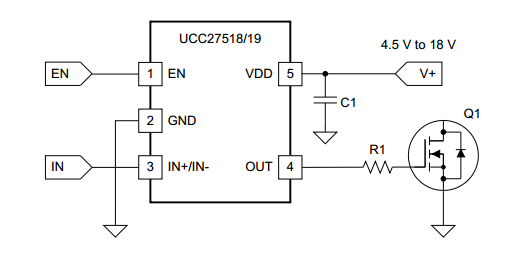
The UCC27518 and UCC27519 single-channel, high-speed, low-side gate driver device is capable of effectively driving MOSFET and IGBT power switches. Using a design that inherently minimizes shoot-through current, UCC27518 and UCC27519 are capable of sourcing and sinking high, peak-current pulses into capacitive loads offering rail-to-rail drive capability and extremely small propagation delay typically 17 ns.

The UCC27518 and UCC27519 provide 4-A source, 4-A sink (symmetrical drive) peak-drive current capability at VDD = 12 V. The UCC27518 and UCC27519 are designed to operate over a wide VDD range of 4.5 V to 18 V and wide temperature range of -40°C to 140°C. Internal Under Voltage Lockout (UVLO) circuitry on VDD pin holds output low outside VDD operating range.
Circuit Project: 4A High-Speed Low-side Gate Driver
Features
  • Low-Cost, Gate-Driver Device Offering Superior Replacement of NPN and PNP Discrete Solutions
  • Pin-to-Pin Compatible With TI’s TPS2828 and the TPS2829
  • 4-A Peak Source and 4-A Peak Sink Symmetrical Drive
  • Fast Propagation Delays (17-ns typical)
  • Fast Rise and Fall Times (8-ns and 7-ns typical)
  • 4.5-V to 18-V Single Supply Range
  • Outputs Held Low During VDD UVLO (ensures glitch free operation at power-up and power-down)
  • CMOS Input Logic Threshold (function of supply voltage with hysteresis)
  • Hysteretic Logic Thresholds for High Noise Immunity
  • EN Pin for Enable Function (allowed to be no connect)
  • Output Held Low when Input Pins are Floating
  • Input Pin Absolute Maximum Voltage Levels Not Restricted by VDD Pin Bias Supply Voltage
  • Operating Temperature Range of -40°C to 140°C
  • 5-Pin DBV Package (SOT-23)
Device Uses
  • Switch-Mode Power Supplies
  • DC-to-DC Converters
  • Companion Gate Driver Devices for Digital Power Controllers
  • Solar Power, Motor Control, UPS
  • Gate Driver for Emerging Wide Band-Gap Power Devices (such as GaN)


Source by http://www.extremecircuits.net/2012/08/circuit-project-4a-high-speed-low-side.html
Read More..

TV Remote Control Jammer

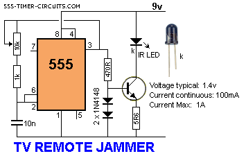
This circuit confuses the infra-red receiver in a TV. It produces a constant signal that interferes with the signal from a remote control and prevents the TV detecting a channel-change or any other command. This allows you to watch your own program without anyone changing the channel !!    The circuit is adjusted to produce a 38kHz signal. The IR diode is called an Infra-red transmitting Diode or IR emitter diode to distinguish it from a receiving diode, called an IR receiver or IR receiving diode. (A Photo diode is a receiving diode).

Circuit Project: TV REMOTE CONTROL JAMMER Circuit

There are so many IR emitters that we cannot put a generic number on the circuit to represent the type of diode. Some types include: CY85G, LD271, CQY37N (45¢), INF3850, INF3880, INF3940 (30¢). The current through the IR LED is limited to 100mA by the inclusion of the two 1N4148 diodes, as these form a constant-current arrangement when combined with the transistor and 5R6 resistor.
Read More..

Zapper Refurbisher Ni Cad Battery Circuit Diagram

Zapper Refurbisher Ni-Cad Battery Circuit Diagram. Batteries and Nickel Cadmium, or simply Ni-Cad NiCad NiCd or sometimes do not work as expected, has no voltage or current, can not be recharged, it means that the battery is internally shorted or partially damaged. You can retrieve this battery in many ways, either by chemical or electrical recovery. One is simpler and recondition the Ni-Cad battery using a zapper circuit.

This circuit restores the Ni-Cad battery short circuit, forcing a high current flow to burn the dirt inside. The resistance of 120 ohm per 10W is used to limit the load current of the capacitor. After zapping the battery goes to the load position, the charging process will take a long time and is indicated by the LED, which will gradually increase the brightness intensity until stable, so when the battery is fully charged.

The power supply for the circuit can be made ​​from a small transformer 350 mA to 1 A with a half-wave rectifier or full wave.

Zapper Refurbishes Ni-Cad Battery Circuit Diagram

Zapper Refurbisher Ni-Cad Battery Circuit Diagram

Read More..

TV Remote Jammer Using 555 IC Circuit Diagram

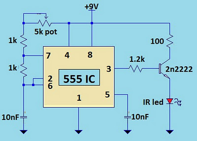
The TV remote control transmits television signals as pulses of frequency around 37.5kHz. Each button on the remote control is pressed or equivalent has a pulse signal codes. This remote transmits pulses of the circuit block of the same frequency as the remote to your TV confuse decoding the transmitted signal.

The heart of the circuit is the 555 timer IC in astable circuit works mode.The output series of pulses at a frequency of 18 kHz to 48 kHz by simply adjusting the 5K potentiometer. What you do is adjust the potentiometer until frequeny jives to its distance from the TV or until the signal is ignored by television.

 TV Remote Jammer Using 555 IC Circuit Diagram

 TV Remote Jammer Using 555 IC Circuit Diagram


Read more IC Circuits
Read More..

Simple Stereo VU Meter

I like to see lights move to music. This project will indicate the volume level of the audio going to your speakers by lighting up LEDS. The LEDS can be any color so mix them up and really make it look good. The input of the circuit is connected to the speaker output of your audio amplifier. You want to build two identical units to indicate both right and left channels. The input signal level is adjusted by the 10k ohm VR. If you wish to make a very large scale model of this unit and hang it on your wall there is an optional output transistor that can drive many LEDS at once. The unit I built drove three LEDS for each output. The sequence of the LEDS lighting are as follows Pin 1, 18, 17, 16, 15, 14, 13, 12, 11, 10.


Read More..

High Performance Interruption Detector

High-Performance Interruption Detector. The circuit presented here detects interruption in security systems. Its features include no false triggering by external factors (such as sun-light and rain), easy relative positioning of the sensors and alignment of the circuit, high sensitivity, and reliability. The circuit comprises three sections, namely, transmitter, receiver, and power supply. The transmitter generates modulated IR signals and the receiver detects the change in IR intensity. Power supply provides regulated +5V to the transmitter and the receiver. 

The power supply and the speaker are kept inside the premises while the transmitter and the receiver are placed oppo site to each other at the entrance where the detection is needed. Three connections (Vcc, GND, and SPKR) are needed from the power supply/speaker to the receiver section, while only two connections (Vcc and GND) are required to the transmitter. The transmitter is basically an astable multivibrator configured around NE555 (IC3). Its frequency should match the frequency of the detector/sensor module (36 kHz for the module shown in figure) in the receiver. The transmitter frequency is adjusted by preset VR2. For making the duty cycle less than 50 per cent, di-ode 1N4148 is connected in the charging path of capacitor C7. 

The output of astable multivibrator modulates the IR signal emitted from IR LEDs that are used in series to obtain a range of 7 metres (maximum). To increase the range any further, the transmitted power has to be raised by using more number of IR LEDs. In such a case, it is advisable to use another pair of IR LEDs and 33-ohm series resistor in parallel with the existing IR LEDs and resistor R5 across points X and Y. The receiver unit consists of a monostable multivibrator built around NE555 (IC2), a melody generator, and an IR sensor module. The output of the IR sensor module goes high in the standby mode or when there is continuous presence of modulated IR signal.
High-Performance Interruption Detector Circuit diagram :
High-Performance-Interruption-Detector-Circuit-Diagram
High-Performance Interruption Detector Circuit Diagram
 
When the IR signal path is blocked, the output of the sensor module still re-mains high. However, when the block is removed, the output of the sensor module briefly goes low to trigger monostable IC3. This is due to the fact that the sensor module is meant for pulsed operation. Thus interruption of the IR path for a brief period gives rise to pulsed operation of the sensor module. Once monostable IC2 gets triggered, its output goes high and stays in that state for the duration of its pulse width that can be controlled by preset VR1. The high output at pin 3 of the monostable makes the musical IC to function. Voltage divider comprising R2 and R3 reduces the 555 output voltage to a safer value (around 3V) for UM66 operation. The du-ration of the musical notes is set by pre-set VR1 as stated earlier. 

For proper operation of the circuit, use 7.5V to 12V power supply. A battery backup can be provided so that the circuit works in the case of power failure also. Potmeter VR3 serves as a volume control. The transmitter, receiver, and power supply units should be assembled separately. The transmitter and the receiver should have proper coverings (booster) for protection against rain. The length of the wire used for connecting the IR sensor module and IR LEDs should be minimum. 

Note. 
 
The heart of the circuit is the IR sensor module (usually used in VCRs and TVs with remote); the circuit works satisfactorily with various makes of sensors. The entire circuit can be fixed in the same cabinet if the connection wires to the sensors are smaller than 1.5 meters. The reflection property of IR signals can also be used for small distance coverage.
Read More..

Build 12V to 9V DC Converter

To get a more precise output voltage, replace zener diode Z1 with 10V and R1 with a 1Kilo ohm potentiometer. A Coolrib for Q1 is optional but highly recommended. You can replace Q1 for a more robust type to get more output amps depending on your requirements. Simple circuit to power your 9 volt cassette recorder and other stuff.


Parts List:

R1 = 560 ohm
C1 = 1000uF/40V, Electrolytic
C2 = 10uF/25V, Electrolytic
C3 = 330nF, Ceramic
Z1 = 9.1V, 1watt zener
Q1 = ECG184, NTE184 
Read More..