Showing posts with label monitor. Show all posts

Thursday, October 23, 2014

Motobike Battery Monitor


A circuit for monitoring the status of the battery and generator is undoubtedly a good idea for motorcyclists, as for other motorists. However, not every biker is willing to drill the necessary holes in the cockpit for the usual LED lamps, or to screw on an analogue accessory instrument. The circuit shown here manages to do its job with a single 5-mm LED, which can indicate a total of six different conditions of the onboard electrical system. This is done using a dual LED that can be operated in pulsed or continuous mode (even in daylight). Built on a small piece of prototyping board and fitted in a mini-enclosure, the complete circuit can be tucked inside the headlamp housing or hidden underneath the tank.

The heart of the circuit is IC2, a dual comparator. The comparator circuit is built without using any feedback resistors, with the indication being stabilised by capacitors C4 and C5 instead of hysteresis. Small 10-µF tantalum capacitors work well here; 220-µF ‘standard’ electrolytic capacitors are only necessary with poorly regulated generators. Voltage regulator IC1 provides the reference voltage for IC2 via voltage divider R2/R3. The onboard voltage is compared with the reference voltage via voltage dividers R4 /R5 and R6/R7, which are connected to the inverting and non-inverting comparator sections, respectively.


Using separate dividers allows the threshold levels to be easily modified by adjusting the values of the lower resistors. IC2a drives the anode of the red diode of LED D4 via pull-up resistor R10. The anode of the green diode is driven by IC2b and R11. T2 pulls R11 to ground, thereby diverting the operating current of the green diode of the LED, if the voltage of the electrical system exceeds a threshold level of 15 V (provided by Zener diode D3). The paralleled gate outputs on pins 10 and 11 of IC3 perform a similar task. However, these gates have internal current limiting, so they can only divert a portion of the current from the red diode of the LED.

Table Power SupplyThe amount of current diverted depends on the battery voltage. The two gates are driven by an oscillator built around IC3a, which is enabled via voltage divider R14/R15 and transistor T1 when the battery voltage is sufficiently high. Depending on the state of IC3a, the red diode of the LED blinks or pulses. The circuit is connected to the electrical system via fuse F1 and a low-pass filter formed by L1 and C1. If you cannot obtain a low-resistance choke, a 1-Ω resistor can be used instead. In this case, the values of C3, C4 and C5 should be increased some-what, in order to help stabilise the indication. D1 protects the circuit against negative voltage spikes, as well as offering protection against reverse-polarity connection. Due to its low current consumption (less than 30 mA), the circuit could be connected directly to the battery, but it is better to power it from the switched positive voltage.
Read More..

Wednesday, October 22, 2014

Wireless Baby Monitor

Walkie-talkies (also known as handheld or PMR, Personal Mobile Radio) can be bought at low prices even from department stores, and they can be operated without a licence in many countries. Considering the low cost, such a set would be very suitable for use as a wireless baby monitor, with the addition of several external components. These are connected to the jack sockets for an external loudspeaker/microphone and an external PTT (Push-To-Talk) switch, which are often found on these devices. 

Project Image :
Wireless Baby Monitor Image
Wireless Baby Monitor Project Image

The walkie-talkie with the extra electronics and microphone is placed in the baby’s room. When the PTT switch on the other walkie-talkie is actuated for about a second the ‘baby’ walkie-talkie produces a series of tones, which the external electronics can detect. This then activates its own PTT switch for about 5 seconds, so it switches over to transmit. During this time the other device can hear what the external microphone picks up. 

Circuit Diagram :
Wireless Baby Monitor-Circuit-Diagram
Figure 1-Wireless Baby Monitor Circuit Diagram

Figure 1 shows the circuit that the author designed for this. It has been designed specifically for a Tevion 3000 PMR sold some time ago by Aldi. This type of PMR has a combined jack socket that includes all the required connections. 

The voltage present on the PTT connector is used to generate the supply voltage for the circuit via R3, D1 and C1/C2. When the loud-speaker output presents a series of tones (when the PTT switch on the other walkie-talkie is held down), it causes T1 to conduct. This also turns on T2 and T3, so that the external microphone is connected to ground. The resulting current that f lows through the microphone should be sufficient to activate the PTT circuit in the walkie-talkie, causing it to transmit. If the external microphone doesn’t draw sufficient current, a resistor (R8) should be connected in parallel. Some experimentation with the value of this resistor may be required. If you want to make use of the internal microphone then R8 should be replaced with a wire link. 

Circuit diagram :
Wireless Baby Monitor-Circuit-Diagramwq
Figure 2-Wireless Baby Monitor Circuit Diagram

When the walkie-talkie switches to transmit the built-in amplifier stops producing a signal and T1 turns off. However, since electrolytic capacitor C3 has been charged up in the mean time, transistors T2 and T3 will keep conducting for several seconds until C3 has been almost discharged via R4. In the Elektor labs a simpler version with the same functionality (Figure 2) has been designed for use with a cheaper PMR set that can be obtained from Conrad Electronics (PMR Pocket Comm Active Pair, order number 930444). These walkie-talkies have separate jack sockets for the LS/Mic and PTT connections. 

When there is a call a series of tones is produced that is used to turn on T1 via R3. T1 then activates the PTT function and the microphone amplifier is turned on. How-ever, it ’s not just the audio signal that is used, but also the DC offset produced when the internal output stage is turned on. Both the internal as well as external loudspeaker are driven via an output capacitor of 100 µF. When there is a call it charges up via R3 and the base-emitter junction of T1. If the walkie-talkie is called often there would be a danger that the output capacitor would remain charged and the DC offset of the audio signal would no longer be sufficient to turn on T1. To prevent this, D1 is connected in reverse across the base-emitter junction of T1, pro-viding a discharge path for the output capacitor.

To keep the circuit active for a minimum amount of time the microphone voltage is used to provide an extra base current. This is done by charging C1 via R1. When the transmitter is turned off the microphone and R2/ D1 provide a discharge path for the capacitor. C2 ensures that the circuit won’t react to spikes caused by interference. As can be seen from the second circuit diagram, use is made of two connectors, a 2.5 mm jack plug for an external headset and a 3.5 mm plug for the PTT function. These connectors are particular to the walkie-talkies we used here. With other types of walkie-talkie you should first check the connection details of the connectors before you connect the circuit up. 

When the circuit is used as a baby monitor you should check that the microphone you’re using can pick up all the sounds. In our case the microphone didn’t appear to be very sensitive. The microphone amplifier has probably been designed for a voice that is near the PMR unit. When used as a baby monitor the microphone should therefore be positioned as close to the baby as possible.


Author : Wolfgang Papke - Ton Giesberts
Read More..

Friday, September 26, 2014

Over Current Mains Monitor Circuit Diagram

Bridge D4-D7 can only provide  the coil voltage for Ret when  the current through D1-D2 exceeds a certain level, because then series capacitor Ci passes the alternating mains 4 current.
Capacitor C1 may need to be dimensioned otherwise than shown to suit the sensitivity of the relay coil. This is readily effected by connecting  capacitors in parallel until the  coil voltage is high enough for  the relay to operate reliably.   

Over Current Monitor Circuit Diagram


Read More..

Wednesday, September 24, 2014

PC Heat Monitor

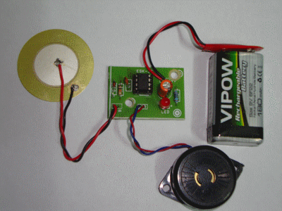
The PC processor generates very high temperature during its operation which is dissipated by the large heat sink placed above the processor. If the heat sink assembly is not tight with the processor or the cooling fan is not working, PC enters into the Thermal shutdown mode and will not boot up. If the PC is not entering into thermal shutdown, the high temperature can destroy the processor. This simple circuit can be placed inside the PC to monitor the temperature near the processor. It gives warning beeps when the temperature near the heat sink increases abnormally. This helps to shutdown the PC immediately before it enters into Thermal shutdown.


Circuit Project: PC Heat Monitor Circuit 
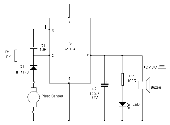
The circuit uses a Piezo element (one used in Buzzer) as the heat sensor. The piezo crystals reorient when subjected to heat or mechanical stress and generates about one volt through the Direct piezoelectric property. IC1 is designed as a voltage sensor with both the inputs tied through the capacitor C1.The non inverting input is connected to the ground through R1 to keep the output low in the standby state. The inputs of IC1 are very sensitive and even a minute change in voltage level will change the output state.
Circuit Project: PC Heat Monitor Circuit
In the standby mode, both the inputs of IC1 are balanced so that output remains low. When the Piezo element accepts heat, it generates a minute voltage which will upset the input balance and output swings high. This triggers LED and Buzzer. Capacitor C2 gives a short lag before the buzzer beeps to avoid false triggering. Warning beep continues till the piezo element cools.
Note: Enclose the circuit inside the PC with the piezo element close to the heat sink of the processor. Adjust the distance between the piezo element and heat sink so as to keep the circuit standby in the normal condition. The piezo element can sense a 10 degree rise in temperature from a distance of 5 cms. Power to the circuit can be tapped from the 12 volt line of SMPS.


Sourced by Dr. Mohn kumar
Read More..

Wednesday, September 10, 2014

AOC A240 WD LCD MONITOR SMPS and BACK LIGHT INVERTER SCHEMATIC

Power Supply_Sub-Power Supply & back-light Inverter Circuit Diagram_AOC Monitor A240WD
SMPS [power Supply Schematic] _ Click on the schematics to Magnify
Sub Power & Back light Inverter

Read More..

Friday, August 8, 2014

Temperature Monitor Wiring diagram Schematic

A simple op-amp schema that will trigger a relay when a preset temperature is reached. Please note that there is no hysteresis in this schema, so that if the temperature changes rapidly, then the relay may switch rapidly.

Temperature Monitor Circuit Diagram

Temperature-Monitor-Circuit-Diagram
Circuit Notes:
This schema uses an ordinary NTC thermistor with a resistance of 47k at room temperature. A suitable part from Maplin Electronics is FX42V. The schema is set in balance by adjusting the the 47k potentiometer. Any change in temperature will alter the balance of the schema, the output of the op-amp will change and energize the relay. Swapping the position of the thermistor and 47k resistor makes a cold or frost alarm.

Calibration:
At room temperature (25 degrees Celsius) a 47k NTC thermistor resistance is approximately 47k. The non-inverting op-amp input will then be roughly half the supply voltage, adjusting the 47k pot should allow the relay to close or remain open. To calibrate the device, the thermistor ideally needs to be at the required operating temperature. If this is for example, a hot water tank, then the resistance will decrease, one way to do this is use a multimeter on the resistance scale, read the thermistors resistance and then set the preset so that the schema triggers at this temperature.

Please note that if the temperature then falls, the relay will de-energize. If the environment temperatures changes rapidly, then the relay may chatter, as there is no hysteresis in this schema.

Hysteresis, allows a small amount of "backlash" to be tolerated. With a schema employing hysteresis, there will be no relay chatter and the schema will trigger at a defined temperature and require a different temperature to return to the normal state. Hysteresis can be applied to the schema using feedback, try a 1Meg resistor between op-amp output, pin 6 and the non-inverting input pin 2 to give the schema hysteresis.

Without offset null adjustment, the output of the 741 IC will be around 2 Volts (quiescent) swinging to nearly full supply when triggered. The 4.7k and 1k resistor form a potential divder so that under quiescent conditions the transistor will be off. Quiescent or steady state means no signal, or in this case (when the temperature does not cause the output to swing to full voltage) 
Read More..