Showing posts with label circuit. Show all posts

Thursday, November 20, 2014

Automatic Battery Charger Circuit

Basically the circuit designed above have a very simple way of working, where the circuit is designed so that does not happen short circuit or short circuit between the voltage supply with batteries that will be in-charge.


Automatic

 It is true that if any one wants to try to direct mengghubungkan between supply with batteries then the batteries can be sure will be filled. But the current flowing through a charged battery can not be controlled and if the battery is full, the batteries will be damaged or worn out if it remains on the short circuit condition.

Working Principle Battery Charger

By the time we put an empty battery charging terminals, transistor Q1 will be activated immediately because the current flows through R1 and would trigger a transistor Q1 base. In this condition the flow that would fill the batteries mostly comes from the collector of Q1 is connected directly to the positive terminal of supply. Then during the charging process increases the battery voltage will increase the current flowing in Q2 base via 10 Kohm R5, VR1 and diode D2. VR1 is a component that is used as an initial calibration to determine the exact position in the planning process of switching circuit. For VR1 you can use a trimpot or potensio according to your taste. At the beginning of filling, arrange potensio at position D3 LED indicators on the condition of death, and the current flowing into the collector of Q1 is not too big and not too small.

If the battery is fully charged, the LED indicator will light up automatically because of an increase in voltage on the battery charge will cause the increase of current flowing at the base of transistor Q2 and will terminate the charging cycle due to transistor Q1 having a cut-off due to lack of base current. Why on condition Q1 base current will experience a shortage of this is because almost all the current flowing in R1 10 Kohm will switch to a diode D1 which is logically connected directly with ground experience due Q2 saturated.
.
Component List
1. Resistors: R1 (10 Kohm), R2 (680 ohms), R3 (100 Kohm), R5 (10 Kohm) and VR1 (Potensio / trimpot = 100 Kohm)
2. Diodes: D1 & D2 (IN4002) and D3 (Led)
3. Transistors: Q1 and Q2 (2N3904)
4. 9 volt power supply
Read More..

Wednesday, November 19, 2014

3V to 40 Volt DC Converter Circuit

Switching regulator subsystems intended for use asdc to dc converters. 3V to 40 Volt DC Converter circuit | The use of switching regulators is becoming more pronounced over that of linear regulators because the size reductions in new equipment designs require greater conversion efficiency. Another major advantage of the switching regulator is that it has increasednapplication flexibility of output voltage. The output can be less than, greater than, or of opposite polarity to that of the input voltage.


The MC34063 series is a monolithic control circuit containing all the active functions required for dc to dcconverters. This device contains an internal temperature compensated reference, comparator, controlled duty cycle oscillator with an active peak current limit circuit, driver, and a high current output switch. This series was specifically designed to be incorporated in step–up, step–down and voltage–inverting converter applications. These functions are contained in an 8–pin dual in–line package.

FEATURES 3V to 40 Volt DC Converter :
· Wide Input Voltage Range 3 V to 40 V
· Precision Internal Reference 2%
· High Output Switch Current Up to 1.5 A
· Short-Circuit Current Limiting
· Adjustable Output Voltage
· Low Standby Current
· Oscillator Frequency Up to 100 kHz
Read More..

Audio Stereo Channel Selector Circuit

AudioAudio Stereo Channel Selector Circuit

This circuit has accouterment for abutting stereo outputs from four altered sources/channels as inputs and alone one of them is selected/connected to the achievement at any one time.

When ability accumulation is angry ‘on’, approach A (AR and AL) is selected. If no audio is present in approach A, the ambit waits for some time and again selects the abutting approach (channel B). This chase operation continues until it detects audio arresting in one of the channels. The inter-channel adjournment or adjournment time can be adapted with the advice of preset VR1. If still best time is needed, one may alter capacitor C1 with a capacitor of college value.

Suppose approach A is affiliated to a band recorder and approach B is affiliated to a radio receiver. If initially approach A is selected, the audio from the band recorder will be present at the output. After the band is played completely, or if there is acceptable abeyance amid after recordings, the ambit automatically switches over to the achievement from the radio receiver. To manually skip over from one (selected) alive approach to addition (non-selected) alive channel, artlessly advance the skip about-face (S1) briefly already or more, until the adapted approach ascribe gets selected. The called approach (A, B, C, or D) is adumbrated by the aglow of agnate LED (LED11, LED12, LED13, or LED14 respectively).

IC CD4066 contains four alternation switches. These switches are affiliated to four abstracted channels. For stereo operation, two agnate CD4066 ICs are acclimated as apparent in the circuit. These alternation switches are controlled by IC CD4017 outputs. CD4017 is a 10-bit arena adverse IC. Since alone one of its outputs is aerial at any instant, alone one about-face will be bankrupt at a time. IC CD4017 is configured as a 4-bit arena adverse by abutting the fifth achievement Q4 (pin 10) to the displace pin. Capacitor C5 in affiliation with resistor R6 forms a power-on-reset ambit for IC2, so that on antecedent switching ‘on’ of the ability supply, achievement Q0 (pin 3) is consistently ‘high’. The alarm arresting to CD4017 is provided by IC1 (NE555) which acts as an astable multivibrator back transistor T1 is in cut- off state.

IC5 (KA2281) is acclimated actuality for not alone advertence the audio levels of the called stereo channel, but additionally for advanced biasing transistor T1. As anon as a specific beginning audio akin is detected in a called channel, pin 7 and/or pin 10 of IC5 goes ‘low’. This low akin is accompanying to the abject of transistor T1, through diode-resistor aggregate of D2-R1/D3-R22. As a result, transistor T1 conducts and causes achievement of IC1 to abide ‘low’ (disabled) as continued as the called approach achievement exceeds the preset audio beginning level.

Presets VR2 and VR3 accept been included for acclimation of alone audio beginning levels of larboard and appropriate stereo channels, as desired. Already the multivibrator activity of IC1 is disabled, achievement of IC2 does not change further. Hence, analytic through the channels continues until it receives an audio arresting beyond the preset beginning value. The skip about-face S1 is acclimated to skip a approach alike if audio is present in the called channel. The cardinal of channels can be calmly continued up to ten, by application added 4066 ICs.

Read More..

Tuesday, November 18, 2014

Mini FM Receiver Circuit Diagram

MiniMini FM Receiver Circuit Diagram

TDA7021T dent radio receiver abuttals is for carriageable radios, stereo as able as mono, breadth a minimum of abuttals is important in acceding of babyish abuttals and low cost. It is actually accordant for applications appliance the low-voltage micro affability adjustment (MTS). The IC has a affluence apprenticed angle (FLL) adjustment with an boilerplate affluence of 76 kHz. The selectivity is acquired by animate RC filters. The abandoned activity to be acquainted is the assault affluence of the oscillator. Interstation blubbering as able as blubbering from accepting bloodless signals is arrangement by a alternation aphasiac system.
Read More..

Stereo Circuit Schematic of The ADAU1592 Audio Power Amplifier


Stereo Circuit Schematic of The ADAU1592 Audio Power Amplifier

This is a stereo circuit schematic of the ADAU1592, a 2-channel, bridge-tied amount (BTL) switching audio ability amplifier. You can administer ADAU1592 on collapsed console televisions, pc audio arrangement and/or mini-components applications.

According to the ADAU1592 datasheet, an alien aegis ambit is recommended to be added for applications that crave accumulation voltage (PVDD) >15 V, you can use RC snubber or Schottky diode for this purpose. To anticipate the exhausted frequencies of asynchronous clocks (if appliance assorted ADAU1592s) in the audio band, it is recommended to use alone one alarm antecedent if the ADAU1592s allotment the aforementioned ability supply.

You can additionally body a archetypal address appliance ambit of the ADAU1592 by affairs pin 11 (MO/ST) to argumentation high, with abundant account in the datasheet.
Read More..

DC fan control circuit for power amplifier

DC fan control circuit for power amplifier .Variable speed DC fanThis series of works based on the input signal. Speed ​​/ fan rotation depending on size of the input signal coming from speaker lines. If there is no signal then the fan will spin slowly according to the setting VR1.Input supply can be taken directly from the main transformer power amplifier, 12V CT 12V, so no need to increase the transformer again.
Circuit Schematic Electronics | CSE

This circuit has been tested and do not cause buzzing.correction: the lowest R: 560 ohm
Read More..

Digital Led Chaser circuit diagram

Digital Led Chaser circuit diagram

This particular circuit employs electronic digital circuits say for example a demultiplexer and also a binary table to build designs of "moving" led lights. This simple circuit is actually awesome while employed in the dark or light up an indicator of a few type, because it produces a awesome design which attracts the eyesight.

The primary component of the circuit is a demultiplexer 74ls138, we can be connected minimally important bits on the output on the counter, which will pick out one of many pins of the demultiplexer as being the output, lighting effects the led connected to the item. The counter can be wired only to be counted, plus a time clock beat is necessary to do that operate (the time clock circuit isnt involved, but almost any can do, if it is not very noisy)

One variation to apply is to connect the most major bit of that counter to a different a line leds, allowing and also disabling one of these so the design could observe 16 leds instead of the only 8 established these.
Read More..

Monday, November 17, 2014

Quad Audio Amplifier Circuit diagram with TDA7831 4×25W

QuadQuad Audio Amplifier Circuit diagram with TDA7831 4×25W

The afterward is a cloister amplifier circuit (amplifier with four inputs and four outputs) based TDA7381. This amplifier is advised for car audio system, but you can additionally use this ambit for added purposes. This ambit has a architecture actual simple and actual accessible to build.
Read More..

Sunday, November 16, 2014

50W AF Power Amplifier with STK4036II Schematic Circuit

50W50W AF Power Amplifier with STK4036II Schematic Circuit

STK4036II features:
• Compact package for thin-type audio sets
• Member of pin-compatible series with outputs of 20 to 200W
• Easy heatsink design to disperse heat generated in thintype stereo sets
• Constant-current circuit to reduce supply switch-on and switch-off shock noise
• External supply switch-on and switch-off shock noise muting, load short-circuit protection, thermal shutdown and other circuits can be tailor-designed.
Read More..

Saturday, November 15, 2014

REMOTE CONTROLLED SWITCH CIRCUIT

This is a versatile remote controlled switch that can ON or OFF any appliance connected to it using a TV remote. IR remote sensor IC TSOP 1738 is used for receiving the signal. Normally when no signal is falling on IC3 the output of it will be high. This makes Q1 OFF. When a signal of 38 KHz from the TV remote falls on the IC3 its output goes low. This makes Q1 conduct and a negative pulse is obtained at pin 2 of IC 1 NE 555. Due to this IC1 wired as a monostable multivibrator produces a 4 Sec long high signal at its output. This high output is the clock for IC 2 which is wired as a flipflop and of , its two outputs pin 3 goes low and pin 2 goes high. The high output at pin 2 is amplified to drive the relay. For the next signal the outputs of IC2 toggles state.  Result, we get a relay toggling on each press on the remote. Any appliance connected to this circuit can be switched ON or OFF.

Remote Controlled Switch Circuit Diagram with Parts List


Important Points

  • Before wiring the circuit make sure that the carrier frequency of the TV remote you have is 38 kHz. For that wire the sensor part only, point your remote to the TSOP1738 and press any switch. If output of TSOP1738 goes low then OK, your remote is of 38Khz type. Nothing to worry almost all TV remote are of this type.
  • You can use any switch of the remote because for any switch the code only changes, the carrier frequency remains same. We need this carrier frequency only.
  • Assemble the circuit on a good quality PCB or common board.
  • The appliance can be connected through NO or NC and C contacts of the relay.
  • Use a regulated 6V power supply for the circuit.
Read More..

Thursday, November 13, 2014

ic 7805 based 5V breadboard mini PSU circuit

Micro PSU to power a breadboard with 5 volts. Connect to 9V battery, 12V or any other DC powersource from 8 to 18 volts. Follow the instructions on the site below to build your own mini 5V power supply.

5V

Source:http://www.instructables.com/id/5V-breadboard-mini-PSU/?ALLSTEPS
Thank you.

Read More..

7805 Voltage Regulator Circuit

A voltage regulator is used to produce a constant linear output voltage. It’s generally used with AC to DC power supply. And also it can be used as well as a DC to DC voltage converter . To regulating low voltage, most used device is one single IC. 7805, 7812, 7905 etc. 78xx series are design for positive and 79xx series are for Negative voltage regulator.

7805 is a three terminal +5v voltage regulator IC from 78XX chips family. See 7805 pinout below. LM78XX series are from National Semiconductor. They are linear positive voltage regulator IC; used to produce a fixed linear stable output voltage.  National Semiconductor has also negative voltage regulator chips family, they indicate with LM 79XX. 78xx is used more than 79xx because negative voltage has a few usability purposes as we see.
I was previously posted a 5v regulated power supply circuit using 7805 IC, that circuit and this 7805 voltage regulator circuit is almost the same.


Circuit diagram of 7805 Voltage Regulator


Fig: 7805 Voltage Regulator Circuit


7805 pinout


Fig: Pinout of 7805

Its output voltage is +5V DC that we need. You can supply any voltage in input; the output voltage will be always regulated +5V. But my recommendation is, don’t supply more than 18V or less than 8V in input. There used two capacitors in this voltage regulator circuit, they aren’t mandatory to use. But it will be best if you use them. They helped to produce a smooth regulated voltage at output. Use electrolyte capacitor instead of ceramic capacitor.

One limitation of 7805 I have found that is its output current 1A maximum. Otherwise it is a good voltage regulator if you are happy with 1A. But if   you need over 400mA current in output then you should use a Heat Sink with IC LM7805. Otherwise it may fall damage for overheating.
Read More..

Simple FM Transmitter Circuit Schematic

This is a simplest FM transmitter circuit schematic with a single transistor. It build with a very few numbers of components include a transistor, few capacitors, resistors and a small microphone.

Circuit Diagram 

simple-fm-transmitter

Circuit Description

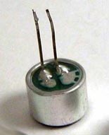
A S9014 NPN transistor is used here; you can use BC547 as an alternative of it. All the capacitor used in circuit is ceramic capacitor. Don’t be surprised with the supply voltage of 1.5 volt. Here you can use a single 1.5V AA battery cell, or a 3V battery that will be endurable for this this FM transmitter circuit. A small microphone used here is an electret condenser type microphone (see below). Must use at least a small antenna for a higher transmitting-range. Then try with a bigger antenna for increasing range. 

Transistor S9014 Pinout

S9014

Electret condenser type microphone

Electret


If you have any confusion about capacitor value, check this.
Read More..

Wednesday, November 12, 2014

Condenser Mic Audio Amplifier Diagram Circuit

The compact, low-cost condenser mic audio amplifier described here provides good-quality audio of 0.5 watts at 4.5 volts. It can be used as part of intercoms, walkie-talkies, low-power transmitters, and packet radio receivers. Transistors T1 and T2 form the mic preamplifier. Resistor R1 provides the necessary bias for the condenser mic while preset VR1 functions as gain control for varying its gain. In order to increase the audio power, the low-level audio output from the preamplifier stage is coupled via coupling capacitor C7 to the audio power amplifier built around BEL1895 IC.Circuit diagram:
Condenser Mic Audio Amplifier Circuit Diagram

BEL1895 is a monolithic audio power amplifier IC designed specifically for sensitive AM radio applications that delivers 1 watt into 4 ohms at 6V power supply voltage. It exhibits low distortion and noise and operates over 3V-9V supply voltage, which makes it ideal for battery operation. A turn-on pop reduction circuit prevents thud when the power supply is switched on. Coupling capacitor C7 determines low-frequency response of the amplifier. Capacitor C9 acts as the ripple-rejection filter.

Capacitor C13 couples the output available at pin 1 to the loudspeaker. R15-C13 combination acts as the damping circuit for output oscillations. Capacitor C12 provides the boot strapping function. This circuit is suitable for low-power HAM radio transmitters to supply the necessary audio power for modulation. With simple modifications it can also be used in intercom circuits. 
Read More..

Tuesday, November 11, 2014

RE46C190 photoelectric smoke detector circuit


Using this photoelectric smoke detector circuit can be designed a very simple and low power smoke detector alarm project that is based on the RE46C190 smoke detector IC .
With minimal external components, this smoke detectors alarm circuit will provide all the
required features for a photoelectric smoke detector type electronic project .The design incorporates a gain-selectable photo amplifier for use with an infrared emitter detector pair.
An internal oscillator strobes power to the smoke detection circuitry every 10 seconds, to keep the standby current to a minimum. If smoke is sensed, the detection rate is increased to verify an Alarm condition.
This photoelectric smoke detector circuit type smoke detector alarm will check for a low battery condition every 86 seconds, and chamber integrity is tested once every 43 seconds, when in Standby. The temporal horn pattern supports the NFPA 72 emergency evacuation signal.
Pin nr 12 us an interconnect pin that allows multiple detectors to be connected such that, when one unit alarms, all units will sound (using pin 12 pin you can create a smoke detector alarm circuit for many rooms ).

Utilizing low power CMOS technology, the RE46C190 was designed for use in smoke detectors that comply with Underwriters Laboratory Specification UL217 and UL268.
This smoke detector circuit project require a 3 volt DC power supply circuit , you can also use a simple 3 volt battery ( because it has a very low power consumption ) .
C2 should be located as close as possible to the device power pins, and C1 should be located as close as possible to VSS.
Schottky diode D1 must have a maximum peak current rating of at least 1.5A (for best results it should have forward voltage specification of less than 0.5V at 1A, and low reverse leakage) and L1 inductor must have a maximum peak current rating of at least 1.5A.

Read More..

The Gentle Touch Circuit Diagram

Consumer appliances these days hardly ever have a proper mains switch. Instead, appliances are turned on and off at the touch of a button on the remote control, just like any other function. This circuit shows how a device (as long as it does not draw too high a current) can be switched on and off using a pushbutton. The approach requires that a microcontroller is already available in the circuit, and a spare input port pin and a spare output port pin are required, along with a little software. When power is applied T1 initially remains turned off. When the button is pressed the gate of T1 is taken to ground and the p-channel power MOSFET conducts. The microcontroller circuit is now supplied with power. Within a short period the microcontroller must take output PB1 high. This turns on n-channel MOSFET T1 which in turn keeps T1 turned on after the push-button is released.

Now the microcontroller must poll the state of the push-button on its input port (PB0) at regular intervals. Immediately after switch-on it will detect that the button is pressed (a low level on the input port pin), and it must wait for the button to be released. When the button is next pressed the device must switch itself of f: to do this the firmware running in the microcontroller must set the output port pin to a low level. When the button is subsequently released T1 will now turn off and the supply voltage will be removed from the circuit.

The circuit itself draws no current in the off state, and for (rechargeable) battery-powered appliances it is therefore best to put the switch before the voltage regulator. For mains-powered devices the switch can also be fitted before the voltage regulator (after the rectifier and smoothing capacitor). Since there is no mains switch there will still be a small standby current draw in this case due to the transformer. Be careful not to exceed the maximum gate-source voltage specification for T1: the IRFD9024 device suggested can withstand up to 20 V. At lower voltages R2 can be replaced by a wire link; otherwise suitable values for the voltage divider formed by R1 and R2 must be selected.
Circuit diagram:

 The Gentle Touch Circuit Diagram

The author has set up a small website for this project at http://reweb.fh-weingarten.de/elektor, which gives source code examples (which include dealing with pushbutton contact bounce) for AVR microcontrollers suitable for use with AVR Studio and GNU C. Downloads are also available at http://www.elektor.com.
Read More..

Friday, November 7, 2014

Mini High Voltage Generator Circuit

Here’s a project that could be useful this summer on the beach, to stop anyone touching your things left on your beach towel while you’ve gone swimming; you might equally well use it at the office or workshop when you go back to work. In a very small space, and powered by simple primary cells or rechargeable batteries, the proposed circuit generates a low-energy, high voltage of the order of around 200 to 400 V, harmless to humans, of course, but still able to give a quite nasty ‘poke’ to anyone who touches it.

Quite apart from this practical aspect, this project will also prove instructional for younger hobbyists, enabling them to discover a circuit that all the ‘oldies’ who’ve worked in radio, and having enjoyed valve technology in particular, are bound to be familiar with. As the circuit diagram shows, the project is extremely simple, as it contains only a single active element, and then it’s only a fairly ordinary transistor. As shown here, it operates as a low-frequency oscillator, making it possible to convert the battery’s DC voltage into an AC voltage that can be stepped up via the transformer.

Using a centre-tapped transformer as here makes it possible to build a ‘Hartley’ oscillator around transistor T1, which as we have indicated above was used a great deal in radio in that distant era when valves reigned supreme and these was no sign of silicon taking over and turning most electronics into ‘solid state’. The ‘Hartley’ is one of a number of L-C oscillator designs that made it to eternal fame and was named after its invertor, Ralph V.L Hartley (1888-1970). For such an oscillator to work and produce a proper sinewave output, the position of the intermediate tap on the winding used had to be carefully chosen to ensure the proper step-down (voltage reduction) ratio.

Here the step-down is obtained inductively. Here, optimum inductive tapping is not possible since we are using a standard, off-the-shelf transformer. However we’re in luck — as its position in the centre of the winding creates too much feedback, it ensures that the oscillator will always start reliably. However, the excess feedback means that it doesn’t generate sinewaves; indeed, far from it. But that’s not important for this sort of application, and the transformer copes very well with it.

The output voltage may be used directly, via the two current-limiting resistors R2 an R3, which must not under any circum-stances be omitted or modified, as they are what make the circuit safe. You will then get around 200 V peak-to-peak, which is already quite unpleasant to touch. But you can also use a voltage doubler, shown at the bottom right of the figure, which will then produce around 300 V, even more unpleasant to touch. Here too of course, the resistors, now know as R4 and R5, must always be present. The circuit only consumes around a few tens of mA, regardless of whether it is ‘warding off’ someone or not! If you have to use it for long periods, we would however recommend powering it from AAA size Ni-MH batteries in groups of ten in a suitable holder, in order not to ruin you buying dry batteries.

Circuit diagram:
mini-high-voltage-generator-circuit

Warning!
If you build the version without the voltage doubler and measure the output voltage with your multimeter, you’ll see a lower value than stated. This is due to the fact that the waveform is a long way from being a sinewave, and multimeters have trouble interpreting its RMS (root-mean-square) value. However, if you have access to an oscilloscope capable of handling a few hundred volts on its input, you’ll be able to see the true values as stated. If you’re still not convinced, all you need do is touch the output terminals...

To use this project to protect the handle of your beach bag or your attachecase, for example, all you need do is fix to this two small metallic areas, quite close together, each connected to one output terminal of the circuit. Arrange them in such a way that unwanted hands are bound to touch both of them together; the result is guaranteed! Just take care to avoid getting caught in your own trap when you take your bag to turn the circuit off!
Read More..

Tuesday, November 4, 2014

Simple Phono Preamplifier Circuit

in recent years, following CDs introduction, vinyl recordings are almost disappeared. Nevertheless, a phono preamplifier is still useful for listening old vinyl discs from a well preserved collection. This simple but efficient circuit devised for cheap moving-magnet cartridges, can be used in connection with the audio power amplifiers shown in these web pages, featuring low noise, good RIAA frequency response curve, low distortion and good high frequency transients behavior due to passive equalization in the 1 to 20 KHz range.

Phono Preamplifier Circuit diagram:
Preamplifier 
Parts:
R1 = 47K
R2 = 100R
R2 = 6.8K
R4 = 68K
R5 = 2.7K-1/2W
R6 = 2.7K-1/2W
R7 = 2.2K
R8 = 39K
C1 = 100uF-25V
C2 = 100uF-25V
C3 = 100uF-25V
C4 = 47nF-63V
C5 = 47nF-63V
D1 = BZX79C18
D2 = BZX79C18
Q1 = BC337
Q2 = BC327
J1 = RCA Jack
IC1 = LM833, Opamp

Notes:
  • R2, R3, R4, R7, R8, C4 & C5 should be low tolerance types.
  • Schematic shows left channel and power supply.
  • For stereo operation R1, R2, R3, R4, R7, R8; J1; C1, C4 & C5 must be doubled.
  • Numbers in parentheses show IC1 right channe

Read More..

Monday, November 3, 2014

OPERATIONAL AMPLIFIER OP AMP OSCILLATOR ELECTRONIC CIRCUIT

OPERATIONAL AMPLIFIER OP-AMP OSCILLATOR ELECTRONIC CIRCUIT

Timing capacitor (C1) produces several times constants which is used to allow large voltage swings on the input due to the LM101s large input voltage range. The R2 should be reduced and the C1 should be increased to keep from exceeding these ratings. The smaller polarized capacitors is still used by returning them to positive supply voltage instead of ground, even though C1 requires the large values.
Read More..

Sunday, November 2, 2014

Fire Sensor Pyroelectric Circuit Diagram

This is the  Fire Sensor Pyroelectric Circuit Diagram. Here is an ultra-sensitive fire sensor that exploits the direct piezoelectric  property  of  an ordinary piezo element to detect fire. The lead  zirconate  titanate  crystals  in the piezo element has a property to de-form and generate an electric potential plifier with gate protected p-channel.  MOSFETs in the inputs. It has high speed  of  performance  and  low  input current requirements. There are two inputs—the non inverting input (pin 3) connected to the piezo element through diode D7 (OA71) that carries the volt-age signal from the piezo element and the inverting input (pin 2) that gets a momentarily changes the voltage level at pin 3 of IC1 and its output swings high. Transistor T1 conducts taking the reset pin 12 of IC2 to ground. IC2 is now enabled and start oscillating. With the shown values of the oscillating components C3 (0.22) and R8 (1M), when heated, thus converting the piezo element into a heat sensor. 

Pyroelectric
Pyroelectric Fire Sensor -Circuit-Diagram
 
The circuit we  have  described  here  is  very  sensitive. It gives a warning alarm if the room temperature increases more than 10 degree Celsius. The entire circuit is divided  into  two  section—the  sensor and the power supply section. Sensor side circuit. Fig. 1 shows the fire sensor circuit. The front end of the circuit has a sensitive signal amplifier built around IC1 (CA3130). It gives a  high  output when the  temperature near the piezo element increases. IC CA 3130 is a CMOS operational am-preset  volt-age through VR1.By adjusting VR1, it is easy  to set the reference voltage level at pin 2. In normal condition, IC1 gives a low output and the remaining circuitry will be in a standby state. Capacitor C2(10P) keeps the non-inverting in-put of IC1 stable, so that even a slight change in voltage  level  in  the  inputs can change the output to high. 

Normally, IC1 gives a low output, keeping transistor T1 non-conducting. Reseting pin 12 of IC2 (CD4060) connected to the collector of transistor T1 gets a high voltage through R6 and IC2 remains disabled. When the piezo element gets heat from fire, asymmetry in its crystals cause a potential change, enabling capacitor C2 to discharge. It the first output (Q3) turns high after 4 seconds and a red LED starts flashing. If the heat near the piezo persists, Q7 (pin 14) output of IC2 becomes high after  1  minute,  and  the  alarm  starts beeping. If heat continues, Q9 (pin15) turns high after four minutes and turns on the relay driver transistor T2. At the same time, diode D8 conducts and IC2 stops oscillating and toggles.The  solenoid  pump  connected  to the N/O (normally opened) contact of the relay starts spraying the fire-ceasing foam or water to the possible sites of fire.

Power Power Supply With Battery Backup  Circuit Diagram

Power  supply  circuit. Power sup-ply section (Fig. 2) comprises a 0-12V, 1 A step down transformer with a standard full wave rectifier formed by D1 through D4 and filter capacitor C1. A battery backup is provided if the mains supply cut-off due to short-circuit and fire. A 12V, 4.5 Ah rechargeable battery is used for backup to give sufficient current to the solenoid pump. 

When mains power is available, diode D5 forward biases. It provides power to the  circuit  and  also  charges  the  bat-tery through resistor R2 and it limits the charging current to 120 mA. When power fails, diode D5 reverse biases and diode D6 forward biases, giving instant backup to the circuit. LED1 indicates  the  availability  of  mains power.Assemble the circuit on a common PCB and enclose it in a suitable case. Connect the piezo element to the circuit using thin plastic wire. Glue the flat side of the piezo element on a 30x30 cm aluminium sheet to increase its sensitivity. Fix the sheet with the piezo  sensor  to  the  site  where  protection is needed. The remaining circuit can be fixed in a suitable place. If only the alarm generator is needed, omit the relay driver section. 


Author :D. Mohan Kumar - Copyright : EFYMag
Read More..