Showing posts with label transmitter. Show all posts

Thursday, November 13, 2014

Simple FM Transmitter Circuit Schematic

This is a simplest FM transmitter circuit schematic with a single transistor. It build with a very few numbers of components include a transistor, few capacitors, resistors and a small microphone.

Circuit Diagram 

simple-fm-transmitter

Circuit Description

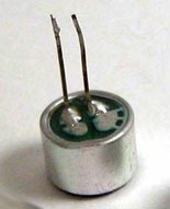
A S9014 NPN transistor is used here; you can use BC547 as an alternative of it. All the capacitor used in circuit is ceramic capacitor. Don’t be surprised with the supply voltage of 1.5 volt. Here you can use a single 1.5V AA battery cell, or a 3V battery that will be endurable for this this FM transmitter circuit. A small microphone used here is an electret condenser type microphone (see below). Must use at least a small antenna for a higher transmitting-range. Then try with a bigger antenna for increasing range. 

Transistor S9014 Pinout

S9014

Electret condenser type microphone

Electret


If you have any confusion about capacitor value, check this.
Read More..

Monday, November 3, 2014

MP3 FM Transmitter

Heres a simple VHF FM transmitter that could be used to play audio files from an MP3 player or computer on a standard VHF FM radio. The circuit use no coils that have to be wound. This FM transmitter can be used to listen to your own music throughout your home. When this FM transmitter used in the car, there is no need for a separate input to the car stereo to play back the music files from your MP3 player.

USB FM Transmitter Project Image

MP3-FM-Transmitter

To keep the circuit simple as well as compact, it was decided to use a chip made by Maxim Integrated Products, the MAX2606 [1]. This IC from the MAX2605-MAX2609 series has been specifically designed for low-noise RF applications with a fixed frequency. The VCO (Voltage Controlled Oscillator) in this IC uses a Colpitts oscillator circuit. The variable-capacitance (varicap) diode and feedback capacitors for the tuning have also been integrated on this chip, so that you only need an external inductor to fix the central oscillator frequency.

t is possible to fine-tune the frequency by varying the voltage to the varicap. Not much is demanded of the inductor, a type with a relatively low Q factor (35 to 40) is sufficient according to Maxim. The supply voltage to the IC should be between 2.7 and 5.5 V, the current consumption is between 2 and 4 mA. With values like these it seemed a good idea to supply the circuit with power from a USB port.

USB FM Transmitter Schematics Circuit Diagram
MP3-FM-Transmitter-Schematic

 Parts List

Resistors 
(all SMD 0805)
R1,R2 = 22kΩ
R3 = 4kΩ7
R4,R5 = 1kΩ
R6 = 270Ω
P1 = 10kΩ preset, SMD (TS53YJ103MR10 Vishay Sfernice, Farnell # 1557933)
P2 = 100kΩ preset, SMD(TS53YJ104MR10 Vishay Sfernice, Farnell # 1557934)
Capacitors (all SMD 0805)
C1,C2,C5 = 4μF7 10V
C3,C8 = 100nF
C4,C7 = 2nF2
C6 = 470nF
Inductors
L1 = 390nF, SMD 1206 (LQH31HNR39K03L Murata, Farnell # 1515418)
L2 = 2200Ω @ 100MHz, SMD, common-mode choke, 1206 type(DLW31SN222SQ2L Murata, Farnell #1515599)
Semiconductors
IC1 = MAX2606EUT+, SMD SOT23-6 (Maxim Integrated Products)
Miscellaneous
K1 = 3.5mm stereo audio jack SMD (SJ1-3513-SMT
CUI Inc, DIGI-Key # CP1-3513SJCT-ND)
K2 = 5-pin header (only required in combination with 090305-I pre-emphasis circuit)
K3 = USB connector type A, SMD (2410 07 Lumberg, Farnell # 1308875)

A common-mode choke is connected in series with the USB connections in order to avoid interference between the circuit and the PC supply. There is not much else to the circuit. The stereo signal connected to K1 is combined via R1 and R2 and is then passed via volume control P1 to the Tune input of IC1, where it causes the carrier wave to be frequency modulated. Filter R6/C7 is used to restrict the bandwidth of the audio signal. The setting of the frequency (across the whole VHF FM broadcast band) is done with P2, which is connected to the 5 V supply voltage.

The PCB designed uses resistors and capacitors with 0805 SMD packaging. The size of the board is only 41.2 x 17.9 mm, which is practically dongle-sized. For the aerial an almost straight copper track has been placed at the edge of the board. In practice we achieved a range of about 6 metres (18 feet) with this. There is also room for a 5-way SIL header on the board. Here we find the inputs to the 3.5 mm jack plug, the input to P1 and the supply voltage. The latter permits the circuit to be powered independently from the mains supply, via for example three AA batteries or a Lithium button cell. Inductor L1 in the prototype is a type made by Murata that has a fairly high Q factor: minimum 60 at 100 MHz.

USB FM Transmitter PCB Layout 

MP3-FM-Transmitter-PCB-Layout

Take care when you solder filter choke L2, since the connections on both sides are very close together. The supply voltage is connected to this, so make sure that you don’t short out the USB supply! Use a resistance meter to check that there is no short between the two supply connectors before connecting the circuit to a USB port on a computer or to the batteries.

P1 has the opposite effect to what you would expect (clockwise reduces the volume), because this made the board layout much easier. The deviation and audio bandwidth varies with the setting of P1. The maximum sensitivity of the audio input is fairly large. With P1 set to its maximum level, a stereo input of 10 mVrms is sufficient for the sound on the radio to remain clear. This also depends on the setting of the VCO. With a higher tuning voltage the input signal may be almost twice as large (see VCO tuning curve in the data sheet). Above that level some audible distortion becomes apparent. If the attenuation can’t be easily set by P1, you can increase the values of R1 and R2 without any problems.

Measurements with an RF analyzer showed that the third harmonic had a strong presence in the transmitted spectrum (about 10 dB below the fundamental frequency). This should really have been much lower. With a low-impedance source connected to both inputs the bandwidth varies from 13.1 kHz (P1 at maximum) to 57 kHz (with the wiper of P1 set to 1/10). In this circuit the pre-emphasis of the input is missing. Radios in Europe have a built-in de-emphasis network of 50 μs (75 μs in the US). The sound from the radio will therefore sound noticeably muffled. To correct this, and also to stop a stereo receiver from mistakenly reacting to a 19 kHz component in the audio signal, an enhancement circuit Is published elsewhere in this issue (Pre-emphasis for FM Transmitter, also with a PCB). Author: Mathieu Coustans, Elektor Magazine, 2009

Notice:
The use of a VHF FM transmitter, even a low power device like the one described here, is subject to radio regulations and may not be legal in all countries.


Read More..

Monday, October 27, 2014

Infrared Audio Transmitter

Infrared Audio Transmitter
Using this low cost Project individual can produce AUDIO from tube with no worrying a person. It does not application some wire relating television and headset. all the rage place of couple of wires it uses imaginary Infrared light to transmit audio signals from small screen to earphone. lacking using several lens a range of up to 6 meters is promising. Range can survive extended by using Lenses and Reflectors with IR sensors comprising transmitters and receivers. IR transmitter uses two-stage transistor amplifier to drive two IR leds connected dressed in succession. An audio output transformer is used (in reverse) to pair Audio output from television to the IR transmitter.
Read More..

Saturday, October 25, 2014

RF Transmitter using LM317 Circuit Diagram

This is the simple RF Transmitter using LM317 Circuit Diagram. Already we saw that the LM317 has hundreds of utilities besides a voltage regulator, how in this article of a audio amplifier with the LM317. Now that circuit the LM317 works for transmit radio waves in CW. The transmitter was done by SM0VPO and works very well, only not found the description the coil.


 RF Transmitter using LM317 Circuit Diagram

RF Transmitter using LM317 Circuit Diagram

If you liked this article,Take a few Seconds to Share this and leave comments
Read More..

Wednesday, October 22, 2014

Four Stage FM Transmitter

This FM transmitter circuit uses four radio frequency stages: a VHF oscillator built around transistor BF494 (T1), a preamplifier built around transistor BF200 (T2), a driver built around transistor 2N2219 (T3) and a power amplifier built around transistor 2N3866 (T4). A condenser microphone is connected at the input of the oscillator. 

Four-Stage FM Transmitter Circuits diagram :
Fm
Four-Stage FM Transmitter Circuits Diagram

Working of the circuit is simple. When you speak near the microphone, frequency-modulated signals are obtained at the collector of oscillator transistor T1. The FM signals are amplified by the VHF preamplifier and the pre-driver stage. You can also use transistor 2N5109 in place of 2N2219. The preamplifier is a tuned class-A RF amplifier and the driver is a class-C amplifier. Signals are finally fed to the class-C RF power amplifier, which delivers RF power to a 50-ohm horizontal dipole or ground plane antenna. Use a heat-sink with transistor 2N3866 for heat dissipation. Carefully adjust trimmer VC1 connected across L1 to generate frequency within 88-108 MHz. Also adjust trimmers VC2 through VC7 to get maximum output at maximum range. 

Regulator IC 78C09 provides stable 9V supply to the oscillator, so variation in the supply voltage will not affect the frequency generated. You can also use a 12V battery to power the circuit.

Assemble the circuit on a general-purpose PCB. Install the antenna properly for maximum range. Coils L1 through L5 are made with 20 SWG copper-enamelled wire wound over air-cores having 8mm diameter. They have 4, 6, 6, 5 and 7 turns of wire, respectively.  

EFY note. This transmitter is meant only for educational purposes. use of this transmitter with outdoor antenna is illegal in most parts of the world. The author and EFY will not be responsible for any misuse of this transmitter.


Author : Pradee G.  - Copyright : EFY
Read More..

Saturday, October 18, 2014

Understanding FM transmitter circuit

Wireless FM Transmitter. The site has some explanation on how the circuit works, however Im not sure about a few things, including the electret mic & how the frequency modulation takes place.
The electret microphone has a current of 200uA which changes by +- 3 uA depending on sound waves. This sets the voltage across R1 to 2V and the voltage across the mic to 4 volts. As the sound hits the mic the current through R1 increases slightly reducing the voltage across the mic. Is that what is happening?

This changing voltage is passed on by the coupling cap, C1 to the base of the transistor, which is biased by R2 & R3 to approx 2V. The voltage across R4 with no signal on the mic will be Vb - 0.7 (drop across vbe), 1.3 volts. As the voltage at b changes R4 will change by the same amount. This change in voltage is seen at the base of the tank circuit. And the signals voltage is increased/decreased. Isnt this what happens in AM? As wouldnt the capacitance need to change in order to get Frequency modulation? And if it was amplitude modulation occuring in the FM spectrum, then how would a radio receiver be able to demodulate the signal?

At this point Im not sure what is happening at the capacitor C3, what is that doing? Is it holding CE at a fixed voltage? And is it along with capacitor C2 considered a bypass capacitor? Or do bypass capacitors need to be connected to ground?
Read More..

Circuit diagram 500mW FM PLL transmitter 88 108MHz using LMX3206 – PIC16F870

Circuit diagram 500mW FM PLL transmitter 88-108MHz using LMX3206 – PIC16F870

Circuit diagram 500mW FM PLL transmitter 88-108MHz


500mW PLL FM transmitter 88-108MHz
This PLL transmitter is controlled and the frequency is very stable and can be programmed digitally.
Transmitter will work 88-108 MHz and output power up to 500mW.
With a small change can set the frequency of 50-150 MHz.

The output power is often set to several watts with transistors.
So therefore I decided to build a simple transmitter with great performances.
The frequency of this transmitter can easily be changed by software and space / compress air coil.
This transmitter is the oscillator colpitts. Oscillator is a VCO (voltage controlled oscillator) which is set by the PLL circuit and PIC micro controller.


This oscillator is called the Colpitts oscillator and voltage controlled to achieve the FM (frequency modulation) and PLL control. T1 must be HF transistors to work well, but in this case I use a cheap and common BC817 transistor. LC tank oscillator needs to oscillate properly.
In this case the LC tank consists of L1 with the C1, C2, C3, and varicap BB139.
Coil parallel to the C1 and C2 in series. The same with the varicap and C3.
You may think that L is parallel to the [(C1 / / C2) + (Varicap / / C3)]
C3 will determine the value range VCO. Large value of C3 will be broader in the range VCO can be.

PLL and Microcontroller


Oscillator is made to work as a “Voltage Controlled Oscillator” VCO.
To control the frequency synthesizer circuit LMX 2306 has been added. The PLL circuit has a pickup coil (L2) is connected to pin 6.
This coil should be placed close to the coil L1 to take some of the energy oscillates.
The LMX2306 PLL in to use this frequency to adjust and lock the VCO to the desired frequency.
Systems also need to set the external reference crystal. In this case I use 12.8 MHz.
 pin2 of MX2306 you will find the PLL filter to form a VM that is set voltage of the VCO.
The PLL tries to arrange so that the oscillator frequency Fout kept locked to the desired frequency.
The desired frequency programmed into the PIC EEPROM and clocked into the synthesizer (LMX2306) at power up.
I will below explain how to program the EEPROM to different frequencies.
In the pin14 of your synthesizer control output. In this output you will find a reference frequency for testing.

(I must warn you that the signal is not symmetrical in form. Pulsa positive only a few microseconds, so you will be hard to see on the oscilloscope.) I solved by connecting it to 74HC4020 (14-stage Binary Counter) to input pin 10 Hours. In Q0 (pin 9) you will have a symmetrical square wave with a frequency half since the circuit is a table. In Q1 pin 7 will be divided by 4, see data sheet for more information.

LF input
You want to send audio must be connected to the audio input (left schematic).
Will affect the signal and thus modulate the FM varicap RF carrier frequency.
A potentiometer P1 was added to adjust the depth of modulation (FM Wide or Narrow FM). You may have to play a bit with a value of P1 because it tends to modulate the lot. You may need to add the 500k – 1M potentiometer only. You test and find out for himself.

Buffer stage
Here you find other HF transistors and work in the class C.
Resistor R1 and resistor Re2 regulate the flow of DC. In this case I find that 9.1k will give a good output power and thus equal to 150. If you want to increase the power should be lower Re2. You can add another 150 ohm resistor in parallel.
In the table below I’ll show the output power with different voltages and resistor values of Re2.
I advice you to not run the transmitter with a high output power. Transistor I use is small and tends to be hot.
I advice you to run the unit from the 0 – to 200mW. At the transistor will 500mW pain …* smiles *
At the output you will find a network T. This “filter” will match the transmitter to the antenna impedance output stage.
You have two variables 60pF capacitors to tune the transmitter for best performance.
The antenna I use I a 1 / 4 wave whip antenna (wire) about 75cm long.
Smaller antenna types, but not so good performance as a dipole.
With a dipole you will be more long distance transmitter.
How long can I pass?
It is a very difficult question because the environment affects the transmission distance is very much.
In a city environment with concrete buildings transmitter will send maybe 200m.
I will send a proposed open 2000m.
I did the test and filed with 70mW output power into a “bad” whip antenna is placed in the room I can send 200-300m to a park without a problem.
Read More..

Sunday, October 5, 2014

Wireless Microphone Transmitter Receiver Circuit

L1 is a toroidal core T50-2 with 80 turns, 0.2mm Ø. L2 requires a 10-20cm ferrite bar, L2a has 3 turns, 0.6mm Ø coiled at ground end of L2b wich has 30 turns, 0.5mm Ø . The current consumption of the wireless transmitter is 150mA and is to be used with wireless headphones receiver. Receiver Section The wireless headphones receiver presented is an standard application of ZN415 produced by Ferranti (short wave receiver). ZN415 assures a quality reproduction, has a 1.5 battery alimentation and contains a MA detector and audio amplifier.  


The current consumption is 5mA, L1 has 40 turns, 0.2 Ø copper and 20mm Ø ferrite. C1 is adjusted with an non metal screw, the reception frequency of this wireless headphone receiver is between 1.7MHz and 3.4MHz – shortwave receiver. This wireless receiver is to be used with wireless headphones transmitter.
Read More..

Friday, September 26, 2014

FTDI Bitbang IR Remote Transmitter Receiver

I use my computer every single minute, I do my work at home and I need to finish lots of paperwork. My computer helps me in almost everything I do. I make sure that my pc is able to do multitasking and functioning well. Just like our body, it should be fit to do all the workload that must be finished within the day.

FTDI Bitbang IR Remote
To come up with another task that a pc can add to its functions, an IR remote was created through an FTDI that receives and transmits data other than the Universal Serial Bus. This is definitely a big help that my pc can easily cope up with simultaneously.

FTDI Bitbang IR Remote
Read More..

Thursday, September 18, 2014

SMD FM Transmitter

Let’s construct a low-power FM transmitter using surface-mount devices (SMD) that will be received with a standard FM radio. Soldering surface mounted devices is not so hard and actually is quite easy. There are many designs for small FM transmitters but they have some problems. First, you need an audio amplifier to get enough modulation. Second, the antenna is attached directly to the collector.

Third, the coil L must be wound by hand and adjusted by stretching. It all ads with a weak signal that tends to drift in frequency. In contrastm the transmitter schematic we present here eliminates some of those problems, using varactor diode for tuning and modulation, givind great sensitivity without an audio amplifier.

FM Transmitter – How it works
The figure below shows the schematic of the transmitter which consists of two stages: an oscillator and an output amplifier. Modulation is from an electret microphone but you can use a low power audio source.

Oscillator stage
Transistor Q1 is a Colpitts oscillator where the frequency is determined by the parallel resonant circuit formed by inductor L, varactor V1 and capacitors C7 and C8. Q1 is a common-collector amplifier where the power gain counts. V1 is actually a dual varactor that eliminate the possibility of forward conduction at the sinewave peaks.

The frequency of oscillation is set by adjusting the DC voltage on V1 with potentiometer R2. R4 and C3 form a low-pass filter to prevent RF from feeding back onto the DC.
Capacitors C7 and C8 form an AC voltage divider to provide feedback at the emitter of Q1 to sustain oscillation. A necessary condition for oscillation to start is for the radio (C7+C8)/C7 to be sufficiently bigger than 1.

SMD transmitter circuit schematic
Frequency Modulation
Modulation is done by superimposing an audio signal from the electret mic onto the DC bias applied to V1. R3 and C1 form a low-pass filter to prevent RF from feeding back to the mic. R3, R4 and R2 form a votage divider for the audio.

Transmitter output stage
The output of the oscillator is fed through C9 to the Q2 emitter-follower. The output of Q2 drives the antenna through C11. The Q2 emitter-follower it ensures that the oscillator is not loaded down by the impedance of the antenna and it provides power gain to drive the antenna.

SMD Transmitter layout
The figure below shows the layout of the PCB and it uses surface-mounted devices like resistors and capacitors (non-polar devices). All the caps are size 0805 and all resistors are size 1206. use through-hole components for Q1, Q2, IC1 and V1. You can use an SOT-89 device for IC1 and an SOT-23 device for V1. Use MPSH10 or a transistor equivalent. Here you can learn how to solder smd chips
The inductor
A coil would consist of two or three turns of wire but for this schematic we will use an inductor with loops of copper on the PCB. Such flat spiral inductor are common at these frequencies.
One formula for flat spiral inductors is:
flat spiral inductors formula where
L = inductance in uH
r = radius of coil (outer radius + inner radius divided by 2 ) inches
N = number of turns
d = depth of coil (outer radius minus inner radius) inches

Tuning range
While commercial FM band goes from about 88 MHz to 108 MHz, the L and C values used in this design allow tuning up to 100 MHz.

Transmitter testing
You will need a portable FM radio and an assistant. First, find an empty spot on the FM dial and set your radio about 30 feet away (9 meters). The radio’s volume control should not be set too high to prevend feedback. Next, power-up your transmitter and talk to yourself as you adjust the frequency with the trim-pot. When your assintant hears you, your transmitter is tuned. You might have to adjust the radio’s tuner slightly for best reception.

Have fun with it but remember that using the transmitter as a bugging device may not be legal in your country. To use the circuit as a wireless microphone, increase the value of R3. The transmitter range is about 100 feet (30 meters) inside a building.
Parts list


Source by : http://www.extremecircuits.net/2012/08/smd-fm-transmitter.html
Read More..

Monday, August 25, 2014

Build a 4 Transistor FM Transmitter Wiring diagram Schematic

 4 Transistor FM Transmitter Circuit Diagram
 
 4 transistor fm transmitter circuit diagram

Build a  4 Transistor FM Transmitter Circuit Diagram. This 4 Transistor FM Transmitter Circuit Diagram provides an FM modulated signal with an output power of around 500mW. The input microphone pre-amp is built around a couple of 2N3904 transistors (Q1/Q2), and audio gain is limited by the 5k preset trim potentiometer. 

The oscillator is a colpitt stage, frequency of oscillation governed by the tank schema made from two 5pF ceramic capacitors and the L2 inductor. The output stage operates as a Class D amplifier, no direct bias is applied but the RF signal developed across the 3.9uH inductor is sufficient to drive this stage. The emitter resistor and 1k base resistor prevent instability and thermal runaway in this stage.
Read More..