Showing posts with label build. Show all posts
Showing posts with label build. Show all posts
Tuesday, November 4, 2014
How to Build a Electronic Telephone Ringer
How to Build a Electronic Telephone Ringer. This circuit produces a ringing sound similar to that made by more recent telephones. It consists of three almost identical oscillators connected in a chain, each generating a squarewave signal. The frequency of each oscillator depends on the RC combination: R4 and C1 around IC1.A, R8 and C2 around IC1.B and R12 and C3 around IC3.C.
The pairs of 100 kΩresistors divide the asym-metric power supply voltage (between 5 V and 30 V) so that, in conjunction with the 100 kΩfeedback resistors (R3, R7 and R11) either one third or two thirds of the supply voltage will be present at the non-inverting inputs to the opamps. The voltage across the capacitor therefore oscillates in a triangle wave between these two values.
The pairs of 100 kΩresistors divide the asym-metric power supply voltage (between 5 V and 30 V) so that, in conjunction with the 100 kΩfeedback resistors (R3, R7 and R11) either one third or two thirds of the supply voltage will be present at the non-inverting inputs to the opamps. The voltage across the capacitor therefore oscillates in a triangle wave between these two values.
Electronic Telephone Ringer Circuit Diagram:
The first oscillator is free-running at a frequency of approximately 1/3 Hz. Only when its output is high, and D1 stops conducting, can the second oscillator run. The frequency of the second oscillator is about 13 Hz, and optional LED D3 flashes when it is running. When the output of the second oscillator is low, the third is allowed to run. The frequency of the third oscillator is around 1 kHz, and this is the tone that is produced. The second oscillator is not absolutely necessary:
its function is just to add a little modulation to the 1 kHz tone. A piezo sounder is connected to the output of the third oscillator to convert the electrical signal into an acoustic one. The current consumption of the circuit is just under 1 mA with a 5V power supply, rising to about 1.65 mA with a supply volt-age of 15 V.

Saturday, October 25, 2014
Build 12V to 9V DC Converter
To get a more precise output voltage, replace zener diode Z1 with 10V and R1 with a 1Kilo ohm potentiometer. A Coolrib for Q1 is optional but highly recommended. You can replace Q1 for a more robust type to get more output amps depending on your requirements. Simple circuit to power your 9 volt cassette recorder and other stuff.

Parts List:
R1 = 560 ohm
C1 = 1000uF/40V, Electrolytic
C2 = 10uF/25V, Electrolytic
C3 = 330nF, Ceramic
Z1 = 9.1V, 1watt zener
Q1 = ECG184, NTE184
Parts List:
R1 = 560 ohm
C1 = 1000uF/40V, Electrolytic
C2 = 10uF/25V, Electrolytic
C3 = 330nF, Ceramic
Z1 = 9.1V, 1watt zener
Q1 = ECG184, NTE184
How To Build Regulated Power Supply with Stability at 3A
The circuit was designed to build a Regulated Power Supply with Stability at 3A will provide a regulated voltage from 40 V to 70 V in a 3 A current.
- 2N3055 – a complementary Silicon Epitaxial-Base planar NPN transistor mounted in Jedec TO-3 metal case for use as power transistor.
- BD243 – an epitaxial-base Silicon NPN transistor intended for wide variety of high speed switching and power amplifier applications such as series and shunt regulators, and driver and output stages of high-fidelity amplifiers.
- BC303 – a PNP silicon planar epitaxial transistor used for AF drivers & outputs, for AF medium power amplifiers, and for switching applications up to 1 A.
There are times when some applications are requiring a regulated power supply that has relatively high output voltage and stability. All of these features are being attained in the design of this circuit. The voltage output of the circuit can range from 40 V up to 60 V while carrying a current of 3 A while providing stabilization. The construction of the circuit is very simple since the components used were available easily in the market. The only thing that matters is how the connection will be ensured.
During the operation, when the circuit is delivering 50 V up to 60 V, the transistor Q1 will be hot enough and would require a large heatsink. For voltage output higher than 50 V up to 70 V, the stability of the circuit may be found unsatisfactory. This is the reason why the ideal output voltage of the circuit is 45 V up to 60 V. In order to alter the output voltage from 40 V up to 70 V, a 470 Ohms potentiometer RV1 is used for the adjustments. However, the potentiometer may also be replaced by two constant resistors with suitable values when the circuit adjustment has been done. This is due to the fact that the use of a potentiometer may lead to a 3 V of over voltage.

As a reminder, the positive output of the circuit should be connected at point A while the 0 V output should be connected at point B. The 0 V reference should not be connected to the ground for the circuit to function properly. the use of this 3 A power supply with an average of 50 V circuit may be found on various applications that normally requires this rating.
Since this type of circuit is easily built, it is being utilized in industrial, educational, clinical, and laboratory facilities. It may come with different additional features such as reduced ripple & noise, overload protection, and short circuit & high current protection.
Since this type of circuit is easily built, it is being utilized in industrial, educational, clinical, and laboratory facilities. It may come with different additional features such as reduced ripple & noise, overload protection, and short circuit & high current protection.
Thursday, October 23, 2014
Build a Converter VGA to BNC Adapter
There are monitors which only have three BNC inputs and which use composite synchronization (‘sync on green’). This circuit has been designed with these types of monitor in mind. As can be seen, the circuit has been kept very simple, but it still gives a reasonable performance. The principle of operation is very straightforward. The RGB signals from the VGA connector are fed to three BNC connectors via AC-coupling capacitors. These have been added to stop any direct current from entering the VGA card. A pull-up resistor on the green output provides a DC offset, while a transistor (a BS170 MOSFET) can switch this output to ground. It is possible to get synchronisation problems when the display is extremely bright, with a maximum green component.
In this case the value of R2 should be reduced a little, but this has the side effect that the brightness noticeably decreases and the load on the graphics card increases. To keep the colour balance the same, the resistors for the other two colors (R1 en R3) have to be changed to the same value as R2. An EXOR gate from IC1 (74HC86) combines the separate V-sync and H-sync signals into a composite sync signal. Since the sync in DOS-modes is often inverted compared to the modes commonly used by Windows, the output of IC1a is inverted by IC1b. JP1 can then by used to select the correct operating mode. This jumper can be replaced by a small two-way switch, if required.
In this case the value of R2 should be reduced a little, but this has the side effect that the brightness noticeably decreases and the load on the graphics card increases. To keep the colour balance the same, the resistors for the other two colors (R1 en R3) have to be changed to the same value as R2. An EXOR gate from IC1 (74HC86) combines the separate V-sync and H-sync signals into a composite sync signal. Since the sync in DOS-modes is often inverted compared to the modes commonly used by Windows, the output of IC1a is inverted by IC1b. JP1 can then by used to select the correct operating mode. This jumper can be replaced by a small two-way switch, if required.

VGA to BNC adapter PCB layout

This switch should be mounted directly onto the PCB, as any connecting wires will cause a lot of interference. The PCB has been kept as compact as possible, so the circuit can be mounted in a small metal (earthed!) enclosure. With a monitor connected the current consumption will be in the region of 30 mA. A 78L05 voltage regulator provides a stable 5 V, making it possible to use any type of mains adapter, as long as it supplies at least 9 V. Diode D2 provides protection against a reverse polarity. LED D1 indicates when the supply is present. The circuit should be powered up before connecting it to an active VGA output, as otherwise the sync signals will feed the circuit via the internal protection diodes of IC1, which can be noticed by a dimly lit LED. This is something best avoided.
Resistors:
R1,R2,R3 = 470Ω
R4 = 100Ω
R5 = 3kΩ3
Capacitors:
C1,C3,C5 = 47µF 25V radial
C2,C4,C6,C7,C10 = 100nF ceramic
C8 = 4µF7 63V radial
C9 = 100µF 25V radial
Semiconductors:
D1 = LED, high-efficiency
D2 = 1N4002
T1 = BS170
IC1 = 74HC86
IC2 = 78L05
T1 = BS170
IC1 = 74HC86
IC2 = 78L05
Miscellaneous:
JP1 = 3-way pinheader with jumper
K1 = 15-way VGA socket (female), PCB mount (angled pins)
K2,K3,K4 = BNC socket (female), PCB mount, 75Ω
Build a Solar power supply
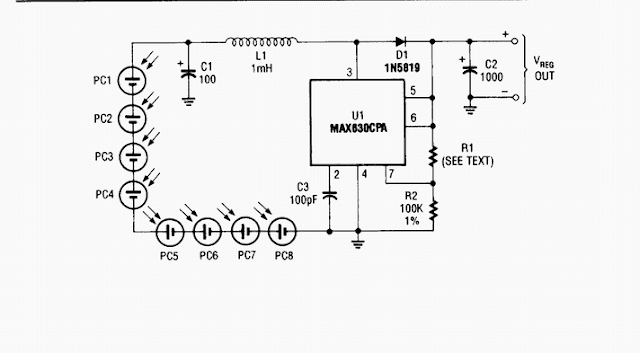
Here is Solar power supply circuit delivers either 4.8 or 7.2 V regulated at 15 mA with a 3-V input from a bank of photocells. Rl should be 453 kQ for a 7.2-V output and 274 РЁ for a 4.8-Vdc output. Regulator efficiency is around 70%. This should be considered when selecting suitable solar cells.
Circuit Diagram
Wednesday, October 22, 2014
Build a 3000W Stereo Power Amplifier Circuit Diagram
How to Build a 3000W Stereo Power Amplifier Circuit Diagram? Lets start first we define 3000wstereo power amplifier circuit diagram this circuit has a power output of up to 1500W RMS power amplifier circuit is often used to power sound systems spelunker for outdor. In the final image can be seen a series of power amplifiers using 10 sets of power transistors for the ending.
This power amplifier circuit using a transistor amplifier from the front, signal splitter, driver and power amplifier. Current consumption required is quite large power amplifier that is 15-20 A 1500W power amplifier circuits for this. Supply voltage needed by the power of this amplifier is the optimal working order symmetrical 130VDC (130VDC-130VDC ground). 1500W amplifier circuit below is a picture series of mono, stereo if you want to make it necessary to make two copies of the circuit. For more details can be viewed directly image the following 1500W power amplifier circuit.
This power amplifier circuit using a transistor amplifier from the front, signal splitter, driver and power amplifier. Current consumption required is quite large power amplifier that is 15-20 A 1500W power amplifier circuits for this. Supply voltage needed by the power of this amplifier is the optimal working order symmetrical 130VDC (130VDC-130VDC ground). 1500W amplifier circuit below is a picture series of mono, stereo if you want to make it necessary to make two copies of the circuit. For more details can be viewed directly image the following 1500W power amplifier circuit.
The series of High Power Amplifier 1500W With Transistor
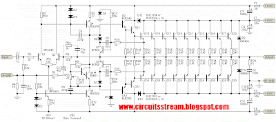
In the above series of power amplifier 1500W is equipped to control a DC Offset function to set the power amplifier is turned on at the moment and with no input signal then the output should be 0VDC. Then also equipped with a flow regulator to the power amplifier bias. Final part of this power amplifier requires adequate cooling to absorb the heat generated. Power amplifier is not equipped with a speaker protector, therefore it is necessary diapsang protector on the speaker output so that when the power amplifier is not the case turned on the beat to the speaker that can damage the speaker.
Monday, October 20, 2014
Build a Single Chip FM Radio Circuit Diagram Using IC TDA 7000
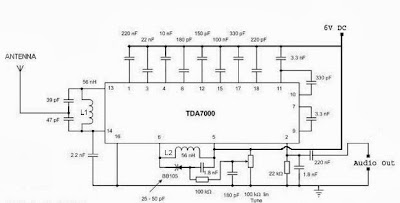
To day i share cheapest cost FM radio circuit using IC TDA 7000. This Single Chip FM Radio Circuit Diagram is designed as per the data sheet and the result is excellent. Ideal for all category of electronic enthusiasts.
The TDA7000 is a monolithic integrated circuit for mono FM portable radios, where a minimum on peripheral components is crucial. The IC TDA 7000 has a Frequency-Locked-Loop system with an intermediate frequency of 70 kHz. The intermediate frequency selectivity is achieved by active RC filters. The only function which needs alignment is the resonant circuit for the oscillator, thus selecting the reception frequency. Spurious reception is avoided by means of a mute circuit, which also eliminates too noisy input signals. Special steps are taken to meet the radiation requirements.
Single Chip FM Radio Circuit Diagram Using IC TDA 7000
Notes
- For L1 and L2 wind 5 turns of 0.6 mm enameled Copper wire on a 4 mm dia plastic former.
- For antenna use a 50mm long insulated copper wire.
- IC TDA 7000 can withstand up to 10 V supply voltage.But I recommend 6V.
- Use an 8 Ohm speaker or Headphone at the audio output.
Thursday, September 4, 2014
Build a Freezer Meltdown Alarm Wiring diagram Schematic
How to Build a Freezer Meltdown Alarm Circuit Diagram? Thats easy or nothing ? This is a simplest schema, This is a schema diagram. The meltdown is a magnet held to a small stand by ice. A reed switch is below the magnet. When the ice melts, the magnet falls on the switch, closing it, and completing the alarm schema.
Freezer Meltdown Alarm Circuit Diagram
Thursday, August 28, 2014
Build a Telephone Conversation Recorder Wiring diagram Schematic
Build a Telephone Conversation Recorder Circuit Diagram. This Telephone Conversation Recorder Circuit Diagram enables automatic switching-on of the tape recorder when the handset is lifted. The tape recorder gets switched off when the handset is replaced. The signals are suitably attenuated to a level at which they can be recorded using the ‘MICIN’ socket of the tape recorder. Points X and Y in the schema are connected to the telephone lines.
Resistors R1 and R2 act as a voltage divider. The voltage appearing across R2 is fed to the ‘MIC-IN’ socket of the tape recorder. The values of R1 and R2 may be changed depending on the input impedance of the tape recorder’s ‘MIC-IN’ terminals. Capacitor C1 is used for blocking the flow of DC. The second part of the schema controls relay RL1, which is used to switch on/off the tape recorder.
Telephone Conversation Recorder Circuit Diagram
A voltage of 48 volts appears across the telephone lines in on-hook condition. This voltage drops to about 9 volts when the handset is lifted. Diodes D1 through D4 constitute a bridge rectifier/polarity guard. This ensures that transistor T1 gets voltage of proper polarity, irrespective of the polarity of the telephone lines.
Tuesday, August 26, 2014
Build a Low Power Consumption 5V Regulator Wiring diagram Schematic
How to build a Low Power Consumption 5V Regulator Circuit Diagram? The special feature of the schema shown below is the low consumption. With voltage n 9 at the entrance and no exit load, absorbs current 50 ma, which is certainly very small compared with a quiescent current 78L05. The components that comprise it are scarce. Just a reference voltage source, formed by the T1 and the IC 1 and an amplifier consisting of the IC2 and T2 so we have to output the desired voltage stabilizer.
The trend that emerges at the output of IC 1 increased to 1,22 V. Using the IC2 and the P1 is set so that the output of the schema is n equal to 5 exactly at the entrance of the schema can be imposed voltage between 6.5 ??? 30 V DC, while the maximum output current reaches 1 mA for the better functioning of the stabilizer, transistors T and T 1 a 1 b should be possible similar characteristics. That is why we preferred a double type transistors MAT02 or alternatively one of the MAT01, SSM2210 or LM394.
Low Power Consumption 5V Regulator Circuit Diagram
If your course is hard to find, you can use two common BC, but which should be selected to have approximately the same threshold voltage. The Operational IC 1 and IC2 is type OR22. Especially for IC2, the peak current of the output can be set using the power introduced in this through the resistor R9. The price of electricity varies between 500 to 400 ma BAC course, before making an increase, you should check whether the output transistor T2 is able to meet the equally elevated currents that it may request the load.
The filter formed by the R6-C 1 is meant to suppress the spurious peaks may accidentally be deployed at the entrance of IC2. The capacitor C2 improves the stability of the schema, wherethose which the stabilizer is required to provide pulsed current. The total schema resistance and is highly therefore sensitive to any kind of electrostatic and magnetic disturbances. The control stabilizer made with a complex load to absorb continuous stream of 1 mA. The pulse of 1 mA Measurement results are shown in the table. The current Ig represents the quiescent current of stabilizer.
Monday, August 25, 2014
Build a 4 Transistor FM Transmitter Wiring diagram Schematic
4 Transistor FM Transmitter Circuit Diagram

Build a 4 Transistor FM Transmitter Circuit Diagram. This 4 Transistor FM Transmitter Circuit Diagram provides an FM modulated signal with an output power of around 500mW. The input microphone pre-amp is built around a couple of 2N3904 transistors (Q1/Q2), and audio gain is limited by the 5k preset trim potentiometer.
The oscillator is a colpitt stage, frequency of oscillation governed by the tank schema made from two 5pF ceramic capacitors and the L2 inductor. The output stage operates as a Class D amplifier, no direct bias is applied but the RF signal developed across the 3.9uH inductor is sufficient to drive this stage. The emitter resistor and 1k base resistor prevent instability and thermal runaway in this stage.
Saturday, August 16, 2014
Build a Semiconductor Failure Alarm Wiring diagram Schematic
Semiconductor failure alarm schema diagram.False alarms produced by semiconductor failure are impossible with this burglar-alarm schema equipped with relays. What`s more, the schema is virtually immune to false triggering. With a standby current of less than 0.1 mA, the schema offers all the features an alarm needs: entry and exit delays, a timed alarm period, and automatic reset after an intrusion.
One CMOS CD4093B quad NAND gate, IC1, supplies both logic and analog timing functions with the aid of Schmitt-trigger switching action. Relays make the schema fail-safe in the alarm-active mode, even when the semiconductors fail. The relays are 12-V, with coil resistances of 250 0 or more. Closing switch S1 initiates schema operation. Capacitor C2 begins charging through resistor R2 and arming indicator LEDllights.
Semiconductor Failure Alarm Circuit Diagram

When pin 2 of IC1a reaches its switching point, its output decreases, extinguishing LEDl and indicating that the exit delay has ended. That output also drives the base of Qllow, so that if the emitter schema completes to the V00 line, Ql conducts. The schema is now armed, and current drain drops to less than 0.1 mA.
When the vehicle is entered, relay RY1 contacts close momentarily, completing the emitter schema of Ql and causing the RY2 contacts to close. Charging C4 through R7 determines the entry-ilelay period. U the system isn`t turned off by opening Sl during this period, the oscillator schema of IC1c and IC1d activates, and a rapid on/off hom-honking cycle kicks on with the aid of Q2 and RY3. The alarm cycle ends after about a minute, when C2 charges through R3 to the threshold voltage of IC1a at pin 1.
This voltage resets the timing schema, readying it for another entry/alarm cycle. RYl is connected for vehicles that use door switches connected to + 12 V. For vehicles that use groundiog door switches, the bottom of the RYl coil should connect to + 12 V instead of ground. In the latter case, the polarity of C7 should be reversed. For home use, the R3C3 time constant should be increased to give a longer alarm.
Subscribe to:
Posts (Atom)