Thursday, November 13, 2014
Simple FM Transmitter Circuit Schematic

Circuit Diagram

Circuit Description
Transistor S9014 Pinout
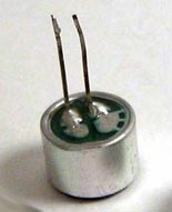
Electret condenser type microphone

Sunday, November 9, 2014
Very Simple Bench Amplifier
Finished project:
Circuit diagram:
The IC works from 4 to 12Volts DC, 12Volt being the maximum recommended value. The internal input impedance of the amplifier is 50K, this is shunted with a 22k log potentiometer so input impedance in this circuit will be lower at about 15k. The input is DC coupled so care must be taken not to amplify any DC from the preceeding circuit, otherwise the loudspeaker may be damaged. A coupling capacitor may included in series with the 22k control to prevent this from happening.
Tuesday, November 4, 2014
Simple Phono Preamplifier Circuit
R1 = 47K
R2 = 100R
R2 = 6.8K
R4 = 68K
R5 = 2.7K-1/2W
R6 = 2.7K-1/2W
R7 = 2.2K
R8 = 39K
C1 = 100uF-25V
C2 = 100uF-25V
C3 = 100uF-25V
C4 = 47nF-63V
C5 = 47nF-63V
D1 = BZX79C18
D2 = BZX79C18
Q1 = BC337
Q2 = BC327
J1 = RCA Jack
IC1 = LM833, Opamp
Notes:
- R2, R3, R4, R7, R8, C4 & C5 should be low tolerance types.
- Schematic shows left channel and power supply.
- For stereo operation R1, R2, R3, R4, R7, R8; J1; C1, C4 & C5 must be doubled.
- Numbers in parentheses show IC1 right channe
Simple Fog Lamp Sensor
Monday, November 3, 2014
Simple Sleeping Aid
Sleeping Aid Circuit diagram :
IC2C and IC2D generate two square waves at about 1.2 and 5 Hz respectively. These wave-forms are converted into 60µS pulses at the same frequencies by means of C5 & C6 and mixed at Q1 Base. This transistor drives the Radiator coil with a scalar series of pulses of 60µS length and 9V amplitude. IC1, IC2A & IC2B form the timer section.
C1 & R2 provide auto-reset of IC1 at switch-on. The internal oscillator of IC1 drives the 14 stage ripple counter and, after about 15 minutes, output pin 1 goes high. Pin 3 of IC2A goes low and stops IC2C & IC2D oscillation. If SW2 is left open (Alternate mode operation), after 15 minutes pin 1 of IC1 goes low, pin 3 of IC2A goes high and oscillators are enabled again.
If SW2 is closed (Stop mode operation), the first time output pin 1 of IC1 goes high, the internal oscillator of the IC is disabled by means of D1. Therefore the circuit remains off until a reset pulse is applied to pin 12 by means of P1 or when the whole device is switched-off and then restarted. The same thing occurs when SW1 is switched on 30 or 60 minutes positions, obviously changing time length.
IC2B drives pilot LED D2 which operates in the following three modes:
- flashes quickly and almost randomly when the Radiator coil is driven
- flashes somewhat slowly and regularly when the Radiator coil is pausing during the Alternate mode operation
- is off when the circuit auto-stops (Stop mode operation)
R1 = 1K 1/4W Resistors
R2 = 10K 1/4W Resistor
R3 = 10M 1/4W Resistors
R4 = 2M2 1/4W Resistors
R5 = 1K 1/4W Resistors
R6 = 10M 1/4W Resistors
R7 = 2M2 1/4W Resistors
R8 = 4K7 1/4W Resistors
R9 = 4K7 1/4W Resistors
C1 = 47µF 25V Electrolytic Capacitors
C2 = 100nF 63V Polyester Capacitor
C3 = 330nF 63V Polyester Capacitors
C4 = 330nF 63V Polyester Capacitors
C5 = 15nF 63V Polyester Capacitors
C6 = 15nF 63V Polyester Capacitors
C7 = 47µF 25V Electrolytic Capacitors
D1 = 1N4148 75V 150mA Diodes
D2 = LED (any type) (see Notes)
D3 = 1N4148 75V 150mA Diodes
D4 = 1N4148 75V 150mA Diodes
D5 = 1N4148 75V 150mA Diodes
IC1 = 4060 14 stage ripple counter and oscillator IC
IC2 = 4093 Quad 2 input Schmitt NAND Gate IC
Q1 = BC327 45V 800mA PNP Transistor
L1 = Radiator coil (see Notes)
P1 = SPST Pushbutton
SW1 = 2 poles 4 ways rotary switch
SW2 = SPST Slider Switch
B1 = 9V PP3 Battery, Clip for PP3 Battery
Features:
- Generates a natural electromagnetic-field
- Makes easier to fall asleep
- Induces a prolonged and sound sleep without drugs
- No side effects
- Select a timing option by means of the rotary switch SW1.
- Choose 15, 30 or 60 minutes operation.
- Select "Stop" or "Alternate" mode operation by means of SW2.
- With SW2 closed (Stop mode operation) the electromagnetic radiation stops after the pre-set time is elapsed.
- With SW2 opened (Alternate mode operation) the device operates for the pre-set time, then pauses for the same amount of time: this cycle repeats indefinitely.
- Place the unit under the pillow and sleep like a log.
- To reset a cycle press P1 pushbutton.
- L1 is obtained by winding randomly 600 turns of 0.2 mm. enameled wire on a 6 mm. diameter, 40 mm. long, steel bolt. Secure the winding with insulating tape.
- Mean current drawing is about 7mA, decreasing to less than 4mA during pauses when in Alternate mode operation.
- Battery life can be dramatically increased omitting LED D2 and its associated resistor R5.
- Use a plastic box to enclose the circuit: metal cases can severely limit electromagnetic radiation.
Wednesday, October 29, 2014
Beat frequency Oscillator Simple Metal Detector Schematic
After assembly, affix the headphones and boring about-face P1. The angle will get lower until it disappears. Continuing to circle P1 in the aforementioned administration will account the angle to acceleration again. The point at witch the angle is the everyman and disappears is alleged “zero beat”. If you can not get this aught exhausted abundance for the absolute about-face of P1 you may accept to baddest altered ethics for C1.
Turn P1 abutting to the aught exhausted position, again move the chase braid abreast a brownish object. The accent should change, depending on the admeasurement and ambit of the metal.
Note that this simple detector’s achievement is not commensurable to added avant-garde bartering products. It will alone ascertain about ample brownish altar at a abbreviate distance. Coins and added baby altar will be abundant harder to find!
Here the Beat-frequency Oscillator Simple Metal Detector Schematic Part List :
- U1: CD4011 (Quad 2-input NAND Gate)
- U2: LM78L05 (5V Regulator IC)
- R1: 2.2k 5% resistor
- R3: 330k 5% resistor
- R4: 270k 5% resistor
- R5: 1k 5% resistor
- C1: 390pF NPO capacitor
- C2, C3: 10nF
- C4: 100nF
- C5: 100uF/16V electrolytic
- C6: 220uF/16V electrolytic
- C7: 100nF ceramic
- P1: 4.7k lin. potentiometer
- L1: 22cm diameter, 14 turns, AWG 26
- K1: SPDT toggle switch
- J1: Headphone jack 1/4 or 1/8 inch
Saturday, October 25, 2014
Simple AM Radio Receiver Diagram Circuit
Circuit diagram:
Copyright: Silicon Chip Electronics
Simple Stereo VU Meter

Simple Electro meter circuit
It can measure up to 30 cm from the target material.
To use this circuit first adjust R2 when the antenna near the material until Amp meter read 1 mA. Link
Simple Audio Peak Detector
Simple DC Fan Controller
The circuit uses an NTC (Negative Temperature Coefficient) Thermister to sense heat. NTC Thermister reduces its resistance when the temperature in its vicinity increases.IC1 is used as a voltage comparator with two potential dividers in its inputs. Resistor R1 and VR1 forms one potential divider connected to the non inverting input of IC1 and another potential divider comprising R2 and the 4.7K Thermister supplying a variable voltage to the inverting input of IC1. VR1 is adjusted so as to give slightly lesser voltage at the non inverting input than the inverting input at room temperature.
DC Fan Controller Circuit

Keep the Thermistor near the heat sink of the Amplifier PCB and switch on the amplifier for 10 minutes. Then adjust VR1 till the Fan stop running.When the temperature rises, Fan will automatically switch on.
Simple Melody Generator Circuit Diagram
R1 = 4.7K
IC = UM66T
Q1 = 2N2222
C1 = 10uF-16v
S1 = On/Off Switch
B1 = 1.5 - 4.5 Battery
SP = 2R Speaker
Notes:
- Power supply must be between 1.5V & 4.5V .Do not exceed 4.5 V.
- Speaker can be driven with external NPN transistor.
- Melody begins from the first note if power is reseted.
- Assemble the circuit on a good quality common board.
Thursday, October 23, 2014
Simple Precision Metronome Pitch generator Circuits Diagram

Parts:
R1__________1M 1/4W ResistorR2_________22K 1/4W ResistorR3__________6K8 1/4W Resistor
R4__________4K7 1/4W Resistor
R5_________47K 1/4W ResistorR6________100K 1/4W ResistorR7_________39K 1/4W ResistorR8_________12K 1/4W ResistorC1_________47pF 63V Ceramic CapacitorC2_______2-22pF 63V Ceramic TrimmerC3________470pF 63V Ceramic CapacitorC4_________10pF 63V Ceramic CapacitorC5________100nF 63V Polyester CapacitorC6________220nF 63V Polyester CapacitorC7_________22µF 25V Electrolytic CapacitorD1-D15___1N4148 75V 150mA DiodesIC1________4060 14 stage ripple counter and oscillator ICIC2________4082 Dual 4 input AND gate ICIC3________4520 Dual binary up-counter ICIC4________4518 Dual BCD up-counter ICIC5________4046 Micropower Phase-locked Loop ICIC6________4040 12 stage ripple counter ICQ1________BC337 45V 800mA NPN TransistorXTAL______2.4576 MHz Miniature Quartz crystal
SW1__________BCD Miniature Thumbwheel Switch (units)
SW2__________BCD Miniature Thumbwheel Switch (tens)
SW3__________BCD Miniature Thumbwheel Switch (hundreds)
SW4_________SPST Slider Switch (On-off)
SW5_________SPDT Slider Switch (Metronome-Pitch)
SPKR_______8 Ohm, 50 mm. Loudspeaker
B1_________9V PP3 Battery
Clip for 9V PP3 Battery
Circuit operation:
CMos IC1 and IC2B quad AND gate form a 2.4576 MHz crystal oscillator plus a 2400 times divider. IC3A provides further division by 16, delivering a 64 Hz stable frequency square wave. This frequency is multiplied (by means of Phase Locked Loop IC5, double decade divider IC4 and IC3B 4 bit binary divider) by the number set by three miniature BCD thumbwheel switches SW1, SW2 and SW3: units, tens and hundreds respectively.Connecting, by means of SW5, Q1 base to pin 2 of IC6, we obtain (after a 64 times division) the same frequency set by thumbwheel switches with quartz precision, and no need for a scale indicator.
Volume regulation of the pitch generator is obtained trimming resistor R5. In the same way, with SW5 set to metronome, the small speaker reproduces the frequency set by thumbwheel switches but divided by 3840, thus obtaining beats per minute ratio.
Wednesday, October 22, 2014
Simple Electrification Unit
The requisite high voltage is generated with the aid of a small mains transformer, whose secondary winding is here used as the primary. This winding, in conjunction with C2, forms a resonant circuit. Capacitor C3 is charged to the supply voltage (12 V) via R3.When a pulse output by IC1b triggers the thyristor, the capacitor is discharged via the secondary winding. The energy stored in the capacitor is, however, not lost, but is stored in the magnetic field produced by the transformer when current flows through it. When the capacitor is discharged, the current ceases, whereupon the magnetic field collapses. This induces a counter e.m.f. in the transformer winding which opposes the voltage earlier applied to the transformer.
Circuit diagram:
This means that the direction of the current remains the same. However, capacitor C2 is now charged in the opposite sense, so that the potential across it is negative. When the magnetic field of the transformer has returned the stored energy to the capacitor, the direction of the current reverses, and the negatively charged capacitor is discharged via D1 and the secondary winding of the transformer. As soon as the capacitor begins to be discharged, there is no current through the thyristor, which therefore switches off. When C2 is discharged further, diode D1 is reverse-biased, so that the current loop to the transformer is broken, whereupon the capacitor is charged to 12 V again via R3. At the next pulse from IC1b, this process repeats itself.
Since the transformer after each discharge of the capacitor at its primary induces not only a primary, but also a secondary voltage, each triggering of the thyristor causes two closely spaced voltage pulses of opposite polarity. These induced voltages at the secondary, that is, the 230 V, winding, of the transformer are, owing to the higher turns ratio, much higher than those at the primary side and may reach several hundred volts. However, since the energy stored in capacitor C2 is relatively small (the current drain is only about 2 mA), the output voltage cannot harm man or animal. It is sufficient, however, to cause a clearly discernible muscle convulsion.
Copyright: Elektor Electronics
Monday, October 20, 2014
Simple Solar Cell Array Charger with Regulator

Simple Programmer AVR Your USB Circuit Diagram

AVR programmer via USB
You can download PCB and various circuit configurations directly from the website http://www.fischl.de/usbasp/.
Scheme
PC connection -> USBasp -> Target Board

Programmer AVR Your USB Circuit Diagram

Simple Auto Power Off
Circuit diagram:
The switch is formed by a p-n-p darlington, T1, which is actuated by push-button switch S1. The very high amplification of the darlington enables it to be kept on fairly long with the aid of a relatively small-value capacitor, C1 (= 100 µF). Resistor R3 limits the charging current of C1 to ensure a long life of S1. Resistors R1 and R2, in conjunction with C1, determine the switch-on time. When this time has elapsed, R1 ensures that T1 is switched off. Since the darlington can handle a UBE of –10 V, a polarity protection diode is not needed.
Copyright: Elektor ELectronics
Saturday, October 18, 2014
Simple Bar Display With Alarm Flasher Schematic

Wednesday, October 1, 2014
Simple LED Voltmeter Circuit
Since this IC is used as a unity gain buffer, the output at pin 6 is equal to the input voltage at pin 3, but at a low impedance. lC2 is connected as a comparator driving a pair of LEDs, D1 and D2. The inverting input samples a portion of the unknown input voltage, whilst the non—inverting input is connected to a 1V reference obtained from the stable voltage across ZD1. ln use RV1 is adjusted till D2 just illuminates. At this point, if the control knob is of the 0 - 10 calibrated type, the pointer will indicate the input voltage. ‘ For example, with SW1 in position 2, and with a reading of 2 on RV1, the input voltage will be 2V. With a little practice, the voltage can be read to 1-2%, comparable to a moving coll instrument. The input lmpedance on all ranges is 3.2M.


Friday, September 26, 2014
Ultra Simple Microphone Preamplifier
The DC, GND and output terminals may be hard wired to the board, you may use PCB pins or a 10-way IDC (Insulation Displacement Connector) and ribbon cable. Power can be anything between +/-9V and +/-18V with an NE5532 opamp. The mic input is electronically balanced, and noise is quite low if you use the suggested opamp. Gain range is from about 12dB to 37dB as shown. It can be increased by reducing the value of R6, but this should not be necessary. Because anti-log pots are not available, the gain control is not especially linear, but unfortunately in this respect there is almost no alternative and the same problem occurs with all mic preamps using a similar variable gain control system.