Thursday, November 13, 2014
ic 7805 based 5V breadboard mini PSU circuit
Micro PSU to power a breadboard with 5 volts. Connect to 9V battery, 12V or any other DC powersource from 8 to 18 volts. Follow the instructions on the site below to build your own mini 5V power supply.
Source:http://www.instructables.com/id/5V-breadboard-mini-PSU/?ALLSTEPS
Thank you.

Sunday, November 2, 2014
12 V AUDIO AMPLIVIER IC TDA7222AP ELECTRONIC DIAGRAM

Pin Name Description
1 Vcc Supply Voltage
2 RR Ripple Reject
3 MC Muting control
4 OP AF Signal Input
5 FB FB Filter
6 GA Gain adjust
7 GND Ground
8 GND Ground
9 OP AF Output
10 BS BootStrap
Tuesday, October 28, 2014
IC TDA7294 50W Power Amplifier with Diagram Circuit
This is a great audio amplifier circuit based on single power IC TDA7294. TDA7294 is intended for use as a high quality audio class AB amplifier in hi-fi applications. It has very low noise and distortion, wide bandwidth and good output current capability, enabling it to supply high power into both 4Ω and 8Ω loads. It has both short circuit and thermal protection, so is quite robust.
Component part list:
R1_____________ 150R R2, R3, R5_____ 10K R4_____________ 680R R6_____________ 22K IC1____________ TDA 7294 Heatsink | C1____________ 1u5F or 1u C2____________ 2n7F C3, C6________ 22uF 63V C4, C5________ 10uF 63V C7, C9________ 2200uF 50V C8, C10_______ 100nF |
With the addition of a handful of parts and a suitable power supply, this module will deliver over 50W RMS into 4 or 8 ohms with <0.1% total harmonic distortion (thd) and <0.1% intermodulation distortion (imd). a similar circuit was published in elektor magazine, 11/96.
It is also suitable as a replacement power amp stage, or upgrade for many existing amplifiers of between 30W-50W, provided they have a suitable dual supply, and most do.
Saturday, October 25, 2014
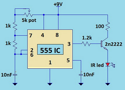
TV Remote Jammer Using 555 IC Circuit Diagram
The heart of the circuit is the 555 timer IC in astable circuit works mode.The output series of pulses at a frequency of 18 kHz to 48 kHz by simply adjusting the 5K potentiometer. What you do is adjust the potentiometer until frequeny jives to its distance from the TV or until the signal is ignored by television.
Friday, October 24, 2014
Police Sirine Circuit with IC 555

Monday, October 20, 2014
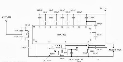
Build a Single Chip FM Radio Circuit Diagram Using IC TDA 7000
Notes
- For L1 and L2 wind 5 turns of 0.6 mm enameled Copper wire on a 4 mm dia plastic former.
- For antenna use a 50mm long insulated copper wire.
- IC TDA 7000 can withstand up to 10 V supply voltage.But I recommend 6V.
- Use an 8 Ohm speaker or Headphone at the audio output.
Friday, September 26, 2014
IC 741 Opamp Parameters Explained
Some important parameters and their significance are mentioned below: Open loop voltage gain Ao: This is the basic voltage gain of the internal circuitry as a whole, and may be expressed as a multiple or in decibels. A typical value of A0 for 741 is 1.00,000 or 100 dB.

Input impedance Zm: This is a measure of the impedance, looking into the input terminals of the op-amp, and is expressed in terms of resistance. A typical value of Zm for 741 is 1 megohm
Output imped¢mce—Zo: Tliis is a measure ot the impe- dance offered by the output terminals of the op-amp. It is also expressed in terms of resistance. A typical value of Zo for 741 is 150 ohms.
Input bias current-Ir: Op-amps utilising bipolar transistor input stages draw a small bias current from the input terminals. A typical value of Ib for 741 is 200 nA (200x 10^-9 amperes).
Input voltage range- Vi(max): This is the maximum value of input voltage that can be connected to the input without causing any damage. It is usually lower than the operating supply voltages. A typical value of Vi(max) for 741 is +/-13V (for the supply voltages +/-15V).
Output voltage range- Vo (max): If the op-amp is over- driven, its output will saturate and be limited by the operating supply voltages. So, Vo(max) is usually specified as being one or two volts less than Vs. A typical value of Vo(max) 741 is +/- 14V (for the supply voltages +/-15V).
Supply voltage range- Vs: Op—amps are usually operated from dual supplies that are anywhere between their minimum and maximum limits. lf the supply voltages are very » high, the op-amp may get damaged. lf they are very low, the op-amp may not work satisfactorily. Typical supply limits for 741 are +/- 6V to +/- 18V.
Differential input offset voltage- Vio: Due to slight imbalances within their input circuitry and due to high gain of the op-amp, it is observed that the output does not register zero voltage even when both inputs are grounded. This small imbalance voltage appearing in the input, which may even cause the output to swing to saturation, is known as the differential input offset voltage. A typical value of Vio for 741 is 2 mV. lt is often required in some particular. op-amp applications to nullify this offset voltage by using external offset nulling circuit, as shown in Fig. (m).
Common mode rejection ratio-CMRR: In an ideal op- amp, if an identical signal is applied to both the inputs, the resultant output is zero. However, in practical op-amps, common mode signals do not entirely cancel out and produce a small signal at the output terminals. The ability of the op-amp to reject common mode signals is usually expressed in terms of common mode rejection ratio. CMMR is the ramp of the op-amp gain with differential signals to the· op-—-amp gain with common mode signals. CMRR value for 741 is typically 90 dB.
Transition frequency-fr: This is the frequency at which the gain of the op-amp falls to unity, Though an op-amp has a very high gain at low frequencies, inthe interest of stability its open loop frequency response is tailored so that the gain falls off as the frequency rises. The gain falls to unity at a transition frequency known as fr. The value of fr for 741 is 1 — MHZ.

Thursday, September 25, 2014
Simplest Automatic Ni Cd Battery Charger Circuit Using IC 555
The circuit uses the timer’s two on-chip comparators, the flip flop and driver amplifier. A zener provides a reference voltage somewhere near the battery voltage with an allowance for adjustment.

The two potential divider networks supply the comparators with adjustable voltages, one for LOW (switch on) and the other for HlGH (switch off). When on, the output gives a maximum of 10V and when off gives GV, the maximum current is 150mA which is limited by the ·47 ohms and protected by the diode. The circuit is calibrated by substituting a variable voltage supply for the Ni-Cd batteries., The HIGH adjustment is set first so that the output switches off at the maximum battery voltage and then the LOW is set for minimum battery voltage. It is simplest to leave the output disconnected from the resistor until after the setting up procedure.
Saturday, September 6, 2014
IC LM12 150 Watts high power amplifier
To supply the required voltage to the amplifier circuit minimum of 7 Volt and a maximum of 24 volts . Incurred sizable ouput for amplifier ic 300 W maximum output.
R1_____________________________________10K
R2_____________________________________10K
R3_____________________________________220K
R4_____________________________________2.2R 2W
C1_____________________________________1uF
C2_____________________________________1000uF
C3_____________________________________68pF
D1_____________________________________BY229
D2_____________________________________BY229
L1_____________________________________4MH
IC1____________________________________LM12
Sunday, August 24, 2014
Stereo Amplifier Circuit with IC AN7142
 |
| This is schematic circuit and i design in simple circuit. Click to view Enlarge |
Tuesday, August 19, 2014
Simple Electronic Combination Lock using IC LS 7220
This is the schema diagram of a simple electronic combination lock using IC LS 7220.This schema can be used to activate a relay for controlling (on & off) any device when a preset combination of 4 digits are pressed.The schema can be operated from 5V to 12V.

To set the combination connect the appropriate switches to pin 3,4,5 and 6 of the IC through the header.As an example if S1 is connected to pin 3, S2 to pin 4 , S3 to pin 5, S4 to pin 6 of the IC ,the combination will be 1234.This way we can create any 4 digit combinations.Then connect the rest of the switches to pin 2 of IC.This will cause the IC to reset if any invalid key is pressed , and entire key code has to be re entered.
When the correct key combination is pressed the out put ( relay) will be activated for a preset time determined by the capacitor C1.Here it is set to be 6S.Increase C1 to increase on time.

For the key pad, arrange switches in a 3X4 matrix on a PCB.Write the digits on the keys using a marker.Instead of using numbers I wrote some symbols!.The bad guys will be more confused by this.
Parts List
C1 1 1uF 25V Electrolytic Capacitor
C2 1 220uF 25V Electrolytic Capacitor
R1 1 2.2K 1/4W Resistor
Q1 1 2N3904 NPN Transistor 2N2222
D1 1 1N4148 Rectifier Diode 1N4001-1N4007
K1 1 12V SPDT Relay Any appropriate relay with 12V coil
U1 1 LS7220 Digital Lock IC
S1-S12 12 SPST Momentary Pushbutton Keypad (see notes)
HD1 1 12 Position Header