Showing posts with label high. Show all posts

Friday, November 7, 2014

Mini High Voltage Generator Circuit

Here’s a project that could be useful this summer on the beach, to stop anyone touching your things left on your beach towel while you’ve gone swimming; you might equally well use it at the office or workshop when you go back to work. In a very small space, and powered by simple primary cells or rechargeable batteries, the proposed circuit generates a low-energy, high voltage of the order of around 200 to 400 V, harmless to humans, of course, but still able to give a quite nasty ‘poke’ to anyone who touches it.

Quite apart from this practical aspect, this project will also prove instructional for younger hobbyists, enabling them to discover a circuit that all the ‘oldies’ who’ve worked in radio, and having enjoyed valve technology in particular, are bound to be familiar with. As the circuit diagram shows, the project is extremely simple, as it contains only a single active element, and then it’s only a fairly ordinary transistor. As shown here, it operates as a low-frequency oscillator, making it possible to convert the battery’s DC voltage into an AC voltage that can be stepped up via the transformer.

Using a centre-tapped transformer as here makes it possible to build a ‘Hartley’ oscillator around transistor T1, which as we have indicated above was used a great deal in radio in that distant era when valves reigned supreme and these was no sign of silicon taking over and turning most electronics into ‘solid state’. The ‘Hartley’ is one of a number of L-C oscillator designs that made it to eternal fame and was named after its invertor, Ralph V.L Hartley (1888-1970). For such an oscillator to work and produce a proper sinewave output, the position of the intermediate tap on the winding used had to be carefully chosen to ensure the proper step-down (voltage reduction) ratio.

Here the step-down is obtained inductively. Here, optimum inductive tapping is not possible since we are using a standard, off-the-shelf transformer. However we’re in luck — as its position in the centre of the winding creates too much feedback, it ensures that the oscillator will always start reliably. However, the excess feedback means that it doesn’t generate sinewaves; indeed, far from it. But that’s not important for this sort of application, and the transformer copes very well with it.

The output voltage may be used directly, via the two current-limiting resistors R2 an R3, which must not under any circum-stances be omitted or modified, as they are what make the circuit safe. You will then get around 200 V peak-to-peak, which is already quite unpleasant to touch. But you can also use a voltage doubler, shown at the bottom right of the figure, which will then produce around 300 V, even more unpleasant to touch. Here too of course, the resistors, now know as R4 and R5, must always be present. The circuit only consumes around a few tens of mA, regardless of whether it is ‘warding off’ someone or not! If you have to use it for long periods, we would however recommend powering it from AAA size Ni-MH batteries in groups of ten in a suitable holder, in order not to ruin you buying dry batteries.

Circuit diagram:
mini-high-voltage-generator-circuit

Warning!
If you build the version without the voltage doubler and measure the output voltage with your multimeter, you’ll see a lower value than stated. This is due to the fact that the waveform is a long way from being a sinewave, and multimeters have trouble interpreting its RMS (root-mean-square) value. However, if you have access to an oscilloscope capable of handling a few hundred volts on its input, you’ll be able to see the true values as stated. If you’re still not convinced, all you need do is touch the output terminals...

To use this project to protect the handle of your beach bag or your attachecase, for example, all you need do is fix to this two small metallic areas, quite close together, each connected to one output terminal of the circuit. Arrange them in such a way that unwanted hands are bound to touch both of them together; the result is guaranteed! Just take care to avoid getting caught in your own trap when you take your bag to turn the circuit off!
Read More..

Wednesday, November 5, 2014

High Level Wideband RF Preamplifier

This High Level Wideband RF Preamplifier can be made in two ways: (1) with the aid of a linear active element, or (2) with a non-linear element operating with negative feed-back. This circuit is of the second kind, using an RF power transistor as the active element. Feedback is also required to ensure correct termination (50 Q) of the aerial, since bipolar transistors normally exhibit a low input impedance. Also, the noise figure is not increased because virtually no signal is lost.

High Level Wideband RF Preamplifier Circuit Diagram:

RF


The common-base amplifier is based on a UHF class A power transistor Type 2N5109 from Motorola. The feedback circuit is formed by RF transformer Th. The input and output impedance of the preamplifier is 50 4 for optimum perform-ance. Network R3-C5  may have to be added to  preclude oscillation outside the pass-band, which  ranges from about 100 kHz to 50 MHz. The gain is  approximately 9.5 dB, the noise figure is between 2  and 3 dB, and the third-order output intercept point  is at least 50 dBm.

The input/output transformer is wound on a Type FT37-75 ferrite core from Micrometals. The input winding is 1 turn, the output winding 5 turns with a tap at 3 turns.

Read More..

Saturday, October 25, 2014

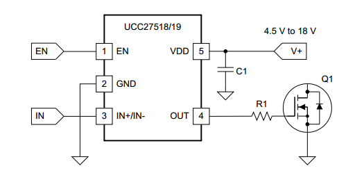
4A High Speed Low Side Gate Driver

The UCC27518 and UCC27519 single-channel, high-speed, low-side gate driver device is capable of effectively driving MOSFET and IGBT power switches. Using a design that inherently minimizes shoot-through current, UCC27518 and UCC27519 are capable of sourcing and sinking high, peak-current pulses into capacitive loads offering rail-to-rail drive capability and extremely small propagation delay typically 17 ns.

The UCC27518 and UCC27519 provide 4-A source, 4-A sink (symmetrical drive) peak-drive current capability at VDD = 12 V. The UCC27518 and UCC27519 are designed to operate over a wide VDD range of 4.5 V to 18 V and wide temperature range of -40°C to 140°C. Internal Under Voltage Lockout (UVLO) circuitry on VDD pin holds output low outside VDD operating range.
Circuit Project: 4A High-Speed Low-side Gate Driver
Features
  • Low-Cost, Gate-Driver Device Offering Superior Replacement of NPN and PNP Discrete Solutions
  • Pin-to-Pin Compatible With TI’s TPS2828 and the TPS2829
  • 4-A Peak Source and 4-A Peak Sink Symmetrical Drive
  • Fast Propagation Delays (17-ns typical)
  • Fast Rise and Fall Times (8-ns and 7-ns typical)
  • 4.5-V to 18-V Single Supply Range
  • Outputs Held Low During VDD UVLO (ensures glitch free operation at power-up and power-down)
  • CMOS Input Logic Threshold (function of supply voltage with hysteresis)
  • Hysteretic Logic Thresholds for High Noise Immunity
  • EN Pin for Enable Function (allowed to be no connect)
  • Output Held Low when Input Pins are Floating
  • Input Pin Absolute Maximum Voltage Levels Not Restricted by VDD Pin Bias Supply Voltage
  • Operating Temperature Range of -40°C to 140°C
  • 5-Pin DBV Package (SOT-23)
Device Uses
  • Switch-Mode Power Supplies
  • DC-to-DC Converters
  • Companion Gate Driver Devices for Digital Power Controllers
  • Solar Power, Motor Control, UPS
  • Gate Driver for Emerging Wide Band-Gap Power Devices (such as GaN)


Source by http://www.extremecircuits.net/2012/08/circuit-project-4a-high-speed-low-side.html
Read More..

High Performance Interruption Detector

High-Performance Interruption Detector. The circuit presented here detects interruption in security systems. Its features include no false triggering by external factors (such as sun-light and rain), easy relative positioning of the sensors and alignment of the circuit, high sensitivity, and reliability. The circuit comprises three sections, namely, transmitter, receiver, and power supply. The transmitter generates modulated IR signals and the receiver detects the change in IR intensity. Power supply provides regulated +5V to the transmitter and the receiver. 

The power supply and the speaker are kept inside the premises while the transmitter and the receiver are placed oppo site to each other at the entrance where the detection is needed. Three connections (Vcc, GND, and SPKR) are needed from the power supply/speaker to the receiver section, while only two connections (Vcc and GND) are required to the transmitter. The transmitter is basically an astable multivibrator configured around NE555 (IC3). Its frequency should match the frequency of the detector/sensor module (36 kHz for the module shown in figure) in the receiver. The transmitter frequency is adjusted by preset VR2. For making the duty cycle less than 50 per cent, di-ode 1N4148 is connected in the charging path of capacitor C7. 

The output of astable multivibrator modulates the IR signal emitted from IR LEDs that are used in series to obtain a range of 7 metres (maximum). To increase the range any further, the transmitted power has to be raised by using more number of IR LEDs. In such a case, it is advisable to use another pair of IR LEDs and 33-ohm series resistor in parallel with the existing IR LEDs and resistor R5 across points X and Y. The receiver unit consists of a monostable multivibrator built around NE555 (IC2), a melody generator, and an IR sensor module. The output of the IR sensor module goes high in the standby mode or when there is continuous presence of modulated IR signal.
High-Performance Interruption Detector Circuit diagram :
High-Performance-Interruption-Detector-Circuit-Diagram
High-Performance Interruption Detector Circuit Diagram
 
When the IR signal path is blocked, the output of the sensor module still re-mains high. However, when the block is removed, the output of the sensor module briefly goes low to trigger monostable IC3. This is due to the fact that the sensor module is meant for pulsed operation. Thus interruption of the IR path for a brief period gives rise to pulsed operation of the sensor module. Once monostable IC2 gets triggered, its output goes high and stays in that state for the duration of its pulse width that can be controlled by preset VR1. The high output at pin 3 of the monostable makes the musical IC to function. Voltage divider comprising R2 and R3 reduces the 555 output voltage to a safer value (around 3V) for UM66 operation. The du-ration of the musical notes is set by pre-set VR1 as stated earlier. 

For proper operation of the circuit, use 7.5V to 12V power supply. A battery backup can be provided so that the circuit works in the case of power failure also. Potmeter VR3 serves as a volume control. The transmitter, receiver, and power supply units should be assembled separately. The transmitter and the receiver should have proper coverings (booster) for protection against rain. The length of the wire used for connecting the IR sensor module and IR LEDs should be minimum. 

Note. 
 
The heart of the circuit is the IR sensor module (usually used in VCRs and TVs with remote); the circuit works satisfactorily with various makes of sensors. The entire circuit can be fixed in the same cabinet if the connection wires to the sensors are smaller than 1.5 meters. The reflection property of IR signals can also be used for small distance coverage.
Read More..

Wednesday, October 22, 2014

High Current Step Up Converter Using MAX641

High Current Step-Up Converter Using MAX641 integrated circuit, manufactured by Maxim IC, can be designed a very simple step-up converter using few electronic components. This step-up high voltage converter electronic projects allows a maximum output current up to 1A.

High Current Step-Up Converter Circuit Diagram

High Current Step-Up Converter Using MAX641

Low battery voltage detector input compare LB1 with internal reference of 1.31 V. LBO output goes in low state when the voltage at pin 1 falls below 1.31 V. The threshold voltage for "low battery", is determined by voltage divider R1-R2.

LED D1 illuminates the LBO output when the input voltage falls below 2.62 V.
Input voltage must remain below 5 V. The maximum effectiveness is 80% conversion.
Read More..

Wednesday, September 24, 2014

High Voltage Generator Circuit Diagram

This is a short  High Voltage Generator Circuit Diagram of a high voltage generator and can be mounted in a small space and powered by rechargeable or simple batteries, the circuit generates a voltage low current but a high turn-on of about 200 to 400 V harmless to humans, of course, but is able to give a pretty nasty shock. 

 High Voltage Generator Circuit Diagram

 High Voltage Generator Circuit Diagram


Here is a project that could be useful this summer on the beach, to prevent anyone touching your things left on your beach towel while you was swimming, you can equally well use it in the office or workshop when you return to work. It operates as a low frequency oscillator, which makes it possible to convert the battery voltage into a DC voltage alternating current that can be enhanced through the transformer. 

Using a transformer with center tap as herein makes possible the construction of a Hartley oscillator transistor T1 around The output voltage can be used directly through R2 and R3 current limiting resistors, which should not in any circumstances be omitted or modified, they are what make the circuit have security. You will then get about 200 V peak-to-peak, which is already quite unpleasant to the touch. 

But you can also use a voltage doubler, shown at the bottom right of the figure, which will produce about 300 V, even more unpleasant to the touch. Here too, of course, the resistance, you know how R4 and R5, should always be present. It can be used in small electric fences, chase away animals, etc.
Read More..

Saturday, September 6, 2014

IC LM12 150 Watts high power amplifier

To supply the required voltage to the  amplifier circuit minimum of 7 Volt and a maximum of 24 volts . Incurred sizable ouput for amplifier ic 300 W maximum output.
high
Part List :
R1_____________________________________10K
R2_____________________________________10K
R3_____________________________________220K
R4_____________________________________2.2R 2W
C1_____________________________________1uF
C2_____________________________________1000uF
C3_____________________________________68pF
D1_____________________________________BY229
D2_____________________________________BY229
L1_____________________________________4MH
IC1____________________________________LM12
Read More..

Tuesday, September 2, 2014

Simple Capacitor Discharge High Voltage Generator Wiring diagram Schematic

Simple Capacitor Discharge High Voltage Generator Circuit Diagram Stepdown transformer T1 drops the incoming line voltage to approximately 48 Vac which is rectified by diode D1; the resultant de charges capacitor C1-through current limiting resistor Rl-to a voltage level preset by R4. When the voltage on R4`s wiper reaches about 8.6 V, Q1 begins to turn on, drawing current through R7 and the base-emitter junction of Q2. 

Q2 turns on and supplies a positive voltage to the gate of silicon-controlled rectifier Q3. The positive gate voltage causes Q3 to conduct, thereby discharging C1 through the primary winding of step-up transformer T2, which results in a high-voltage arc at output terminal X. The voltage developed at T2`s output is determined by the value of C1, the voltage across C1, and the turns ratio of transformer T2. 

The frequency or pulse rate of the high voltage is determined by the resistance of T1 `s primary and secondary windings, the value of R1, and the value of Cl. The lower the value of each item, the higher the output pulse rate; the peak output voltage will only remain unchanged if C1`s value remains unchanged.

Capacitor Discharge High Voltage Generator Circuit Diagram

Capacitor

Read More..

Friday, August 22, 2014

High And Low Voltage Cut Off With Time Delay Wiring diagram Schematics

The power line fluctuations and cut-offs cause damages to electrical appliances connected to the line. It is more serious in the case of domestic appliances like fridge and air conditioners. If a fridge is operated on low voltage, excessive current flows through the motor, which heats up, and get damaged.

The under/over voltage protection schema with time delay presented here is a low cost and reliable schema for protecting such equipments from damages. Whenever the power line is switched on it gets connected to the appliance only after a delay of a fixed time. If there is hi/low fluctuations beyond sets limits the appliance get disconnected. The system tries to connect the power back after the specific time delay, the delay being counted from the time of disconnection. If the power down time (time for which the voltage is beyond limits) is less than the delay time, the power resumes after the delay: If it is equal or more, then the power resumes directly.

This schema has been designed, built and evaluated by me to use as a protector for my home refrigerator. This is designed around readily available semi-conductor devices such as standard bipolar medium power NPN transistor (D313/SL100/C1061), an 8-pin type 741 op-amp and NE555 timer IC. Its salient feature is that no relay hunting is employed. This draw back is commonly found in the proctors available in the market.

The complete schema is consisting of various stages. They are: - Dual rail power supply, Reference voltage source, Voltage comparators for hi/low cut offs, Time delay stage and Relay driver stage. Lets now look at the step-by-step design details.

Dual rail power supply.
This is a conventional type of power supply as shown in Figure 1. The power is applied through the step-down transformer (230/12-0-12V/500mA). The DC proportional to the charging input voltage is obtained from bridge rectifier. Two electrolytics are there to bypass any spikes present. Bridge is capable of handling currents up to 1 Amp.
Output is given by: -
V(out) = 0.71 X V (secondary)
= 0.71 X 24V
= 17.04 V
(This equation is similar for the negative rail as well)

Circuit diagram

Build


Low voltage cut off op-amp
Figure 2 shows the use of very common and easily available op-amp 741 as a comparator. The op-amp is available in TO-5 and DIP type packing.

Circuit diagram

Build


In this ckt the zener diode D1 and it’s associated resistor R1 are connected to the non-inverting terminal (+ve) of 741 to give the suitable reference voltage. The DC voltage from the sensor is given to the inverting (-ve) terminal through pre-set R2.This is used to set the input level.
When the sensor input is less than Zener voltage the output from the Op-amp remains high and when it is greater than Zener voltage the output goes low. When the sensing voltage is equal to Zener voltage the output of the op-amp is approximately zero.
This phenomenon is used as a decision for switching the relay and to give cutoff in a low voltage situation.

High voltage cut off op-amp
Here the op-amp is used as a inverted amplifier. See Figure 3.Zener and resistor network gives reference voltage to the inverting terminal (-ve) of op-amp. Sensing voltage derived through the 10 K pre-set is given to the non- inverting (+ve) terminal and this sets the high level cut.

When the input DC from the sensor is less than Zener voltage the output of the op-amp is low and vice-versa. When the input DC voltage is equal to the zener voltage, the op-amps output is approximately zero.

Circuit diagram

Build


Time delay
I’ve selected the 555 timer due to following reasons.
1. Timing from microseconds through hours.
2. Ability to operate from wide range of supply voltages.
3. High temperature stability.
4. Easily Available.
5. Its triggering schema is quite sensitive.

This is basically a monostable. The external timing capacitor C2 is held initially discharged by the timer. The schema triggers upon receiving a pulse to its pin 2 when the level reaches 1/3 Vcc. Once triggered., the schema will remain in that state until the set time is elapsed or power to the schema cuts off. The delayed period in seconds is 1.1 C2.R1 where R1 is in megohms and C2 is in microfarads. In practice, R1 should not exceed 20 M. If you use an electrolytic capacitor for C2, select a unit for low leakage. The time delay may have to be adjusted by varying R1 to compensate for the wide tolerance of electrolytics.

Circuit diagram

Build


Relay Driver
The output from the voltage level detectors cannot directly drive the relay and hence the relay driver is used.

Circuit diagram

Build


In this a relay (12V <500 ohms) is connected to the collector of NPN transistor. The out put voltage from the comparator is applied to the base of NPN transistor through a resistance R1. When the output from the comparator is low the transistor is in OFF state and the relay is in de-energized state. Similarly when the output from the comparator goes high the transistor switches ON and the flow of current from the collector to emitter of transistor energizes the relay.

Generally in a relay driver schema, parallel to the relay coil, a diode or a capacitor is used. This is to eliminate the back e.m.f generated by the relay coil when currents are suddenly broken. Capacitor C1 is connected in parallel to the coil, which filters out the back emf but it, slows down the working of relay.

A better method is to connect two diodes (as shown in the figure 5) that stop the relay – transistor junction swinging more than 600mV above the positive rail or below the zero-volt rail. During normal operation the diodes are reverse biased and have no effect on the performance of schema. But when back emf is induced, the diodes conduct heavily and absorb all transient voltages. However, I have employed the both methods.
The Complete Circuit

Circuit diagram


Build


Under normal operating conditions i.e. when the input voltage is between maximum and minimum limit the output from the both the comparators are low. The transistor Q1 is OFF and the relay is in de-energized (pole connected to N/C pin) state and the output is obtained.

When the input voltage is below or above the limits set by the pre-sets R8 or R9, the output of the Op-Amps goes either low or high and diodes D1 or D2 would be forward biased depending on the situation. Transistor Q1 switches ON and the flow of current from collector to emitter energizes the relay and the output is cutoff.

A small amount of hystersis has been added via feed back resistors R10 & R11 so that the relay turns on when the level falls to a particular value but does not turn again until it raises a substantial amount above this value. Other wise the relay contacts will frequently turn on/off and produce chattering.

Construction Hints
1) I used a piece of varoboard, which has copper strips on one side to mount the components, and housed the entire schema and the transformer in a discarded ATX PC power supply box.

2) An autotransformer has been used to set the limits. Set the output of the autotransformer to 250V AC and connect it to the primary of transformer T1 (see Figure 1). Then adjust the pre-set R9 such that relay just energizes. This is the high limit. Next set the output of the autotransformer to 200V AC and adjust the pre-set R8 such that the relay energizes. Please note that these are my preferred limits but you may select any range from say 170 to 270V AC.

3) A neon with a suitable resistor could be connected between the AC supply lines as an ON indicator. Alternatively, LED with a current limiting resistor could be connected between the relay coil so when the relay is energized LED will indicate the situation.
Read More..

High Low voltage cut off with delay alarm


This straight forward schema will protect electrical appliances from over voltage as well as under voltage.The schema also produces an alarm when the power supply comes back.An ideal schema for home to protect your valuable equipments from voltage fluctuations.The same schema with some modifications can be used to make a automatic voltage stabilizer


When the mains voltage is in the normal level ,the voltage at the negative terminal of zener diode D4 will be less than 5.6 Volts.At this condition transistor T1 will not conduct.The same time voltage at the negative terminal of zener diode D5 will be greater than 5.6 and so the transistor T2 will be conducting.The relay will be activated and the green LED wil be glowing.

When the mains voltage is higher than the set limit the transistor T1 becomes conducting since the voltage at the negative terminal of D4 is greater than 5.6 V.At the same time transistor T2 will be non conducting which results in the deactivation of relay to cut the mains supply from load.When the mains voltage is less than the set limit transistors T1 & T2 becomes non conducting making the relay to de- activate and cut the load from mains.Ω

The timer NE555 is wired as a monostable multivibrator with a pulse width of 10ms.When the power comes back after a cut off a negative voltage is obtained at the trigger pin which triggers the IC NE555.The transistor T3 gets forward biased and it drives the buzzer to produce a beep as an indication of power resumption.Also the transistor T1 is made on which in turn makes T2 off.As a result the relay will remain de- activate for 10ms and this provides the sufficient delay and the equipment is protected from surge voltages.


Notes.

* To calibrate the schema a autotransformer is needed.Connect the output of autotransformer to the transformer primary.
* Set the voltage to 260V and adjust VR1 to make the relay deactivated.
* Now set the autotransformer to 160V and adjust VR2 so that the relay is de-energized.
* VR3 can be used to vary the volume of buzzer.


Read More..