Sunday, August 31, 2014

Making Home Theater 5 1 Surround Amplifier

5.1
Actually, 5.1 channel amplifier consists of 6 amplifiers 1 channel mono, which has certain specifications on each canals. Has 6 channel surround sound amplifier that consists of Front Left | Center | Front Right | Rear Left (Left Surround) | Rear Right (Right Surround) | and LFE (Subwoofer).


For clarity I give a simple illustration of the layout and the circuit for these speakers.


5.1
5.1 Speaker Setup

Accoustic Field Generator

Acoustic Field Generator is generating acoustic sound with surround effects are adjustable with a standard Dolby Surround, able to produce surround sound is good enough but not too much need of funds. Technological developments as if not only focused on one area alone but on all fronts. The development of technologies that exist today one of them is in the field of audio. With more advanced audio technology today not only as mere entertainment but has become a hobby, hobby is not cheap of course. Many audio enthusiasts trying to make music sound that sounded to be very hard to make music sound as live, the addition of the amplifier, woofer or special speakers that cost is not cheap.

The sound effects are living seems to now is something that most do not have to exist in every good audio devices. This effect is basically a surround effect that can lead to sound as though coming from different directions and his voice can still be heard clearly. Currently Compo-tape tape that has been a lot of these facilities surround sound but not good enough when heard from a considerable distance because of the effects surroundnya missing. This is because the distance is too far listener and speaker, speaker layout is not quite right, or the effect of unfavorable surround.

Surround effects are nice and can be heard with a good surround system is a system that is in movie theaters and to make it not a bit prangkat needed funds. However, if satisfaction remains the number one then the fund is not a major problem. To find a middle ground between price and quality surround effects it was attempted to make the Acoustic Field Generator that can produce surround sound is good enough but not too much need of funds. Acoustic Field Generator is capable of generating acoustic sound with surround effects are adjustable with a standard Dolby Surround.

Accoustic Field Generator Construction


Basically an Acoustic Field Generator built from op-amp circuit and filters. Op-amps are usually used as a voltage amplifier in the Acoustic Field Generator is more widely used as active filters. The filter in the tool is very instrumental in creating an acoustic sound that is really clear, but in practice, almost all the filters, do not miss the precision of the signal with a specific frequency. An op-amp is good for this application is the op-amp which has a wide bandwidth, rise time, slew rate and fast setting timenya. In addition to op-amp and active filter, theres more important parts of the power supply. This is the part that is instrumental in creating excellence acoustic sound because of the bad power supply which is the only producer of noise, which will enter into a voice signal path so that should clear acoustic sound into an acoustic sound with the addition of reverberation (noise). The power supply used is the twin power supply + / - 18 volts DC. Part Acoustic Field Generators

Before we start doing this project, it helps us know in advance about the function of each speaker.

Front Channel

Channel Front is a forward channel input signal LR. LR signal is passed to an amplifier with gain = 1 so that this signal is passed without change / to filter the input signal LR. Front Left and Front Right, is a public speaker that we encountered in stereo amplifier, consisting of a woofer and tweeter. Woofers generally produce low tone sound with a frequency range ranging from 80Hz - 250Hz, while the tweeter produces a high tone with a frequency range between 15kHz - 20kHz. For projects that we will create, its good we use a good quality woofer, with a size of 10 inches and a type piezoelectric tweeter for each speaker fronts.

Front
Front Channel 5.1 Amplifier

Center Channel

Center, the fullrange speakers, which produce sound with a frequency range between 80Hz - 10Khz. Output from the center speaker is a summation of left and right signal (left + right = center). In a movie or song Dolby Surround format, commonly used center for dialogue / vocal or speech of the actor / artist of a film and to produce a sound that moves ahead of us.

Center
Center Channel 5.1 Amplifier


Rear Channel with Surround System

In this section is the core of this hard perangakat. These sections produce surround effects. To produce the surround effect is required special IC MN3005 / 8 and MN3101. Both these ICs will delay the incoming signal in several phases, so that the signal output from this phase will be left with a signal phase of the signal lain.Pada this section L and R are deducted (LR) and then passed in the buffer, filter LPF, delay line, filter LPF (7KHz) and the last is a splitter between the signals R and L. Circuit which causes the surround effect is 75KHz LPF circuit that produces its output fed to the Right Rear 75KHz LPF amplifier input while it diparalel with the Left Rear amplifier input so as to produce two signals L and R which is basically a LR signal a phase lag with the original signal phase.

Rear Left and Rear Right, also known as surround speakers. This speaker is generally a semi-midrange speaker (usually used on television or Mini Compo), commonly called satellite speakers. In a movie surround speakers are used to generate the audible sound of distant voices or sounds that move from the back of our approach. In a music surround speakers produce sound backing vocals and generally sounds like guitars, violins and trumpets sounded clear here.

Rear
Rear Channel 5.1 Amplifier

Subwoofer Channel

Part of this subwoofer is the summation of inputs L and R inputs to a summing amplifier. The output of the summing amplifier is passed to a class 2A LPF which will only pass signals with frequency rendah.Subwoofer, sometimes referred to as LFE (Low Frequency Effect). For these speakers using a subwoofer speaker. Speaker woofer speaker subwoofer is designed specifically to be able to respond to sound with a very low frequency, ranging from 15Hz - 120Hz. For low tone effect can be produced by either (without any harmonic frequency), then the acoustic box / box speakers are also designed specifically with a variety of methods (there are no visible speaker / inside the box, there are that use insulation / labyrinth, etc. ), so that the speaker is capable of compressing the air effectively, so that will feel the effect.

Subwoofer
Subwoofer Channel 5.1 Amplifier


Wiring
Wiring Diagram Home Theater Amplifier / 5.1 Amplifier

Read More..

Car Mobile Phone Charger Circuit

Car
Cellphone battery charging process when were done traveling is a big problem. Because when traveling source of power supply is generally difficult to find. If you turn on your phone then the battery continuously over time will run out within a period of five to six hours and eventually mobile phones unusable. Here is described a series of simple charger that will increase battery life two to three hours.


In principle, the charger uses a series of Limited Voltage Current Source. Generally requires cellphone battery voltage 3.6 - 6 volts DC and currents 180-200 mA to perform the charging process. Cellphone battery usually consists of three NiCd battery cells, and each cell has a voltage of 1.2 volts potential. At the speed - average low flows required to charge mobile phone battery about - about 100mA.

Car

In this series there is a 12V voltage source consists of 8 regular battery cells (each cell 1.5 Volt) able to supply current at 1.8 A which is connected with output terminals.

The circuit is also able to monitor the battery voltage level which is in charge. And will automatically cut off the charging process when the output terminal detects a certain battery voltage level predetermined. Timer IC NE555 is used to charge and monitor the voltage level in the battery, Pin 5 (IC1) as the control voltage using a reference voltage zener voltage 5.6Volt. Voltage at Pin 6 as the threshold set by VR1 and the voltage at Pin 2 as the trigger is set by VR2.

When the cellphone battery is connected in series (the Charging Process) applied voltage on PIN2 (IC1) as a trigger would be below the value 1 / 3 Vcc and will cause the Flip-Flop in IC1 will ON and on Pin 3 (IC1) will be high (Cause transistor T1 saturation.). When the battery is full (Full Charge) then the voltage will rise and the voltage on the PIN2 (IC1) will be above the level of trigger point threshold. This will cause the Flip Flop OFF and the output will be low (transistor T1 causes the cutoff) and indirectly also the charging process will stop.

Pin 6 (Threshold IC1) is set at 2 / 3 Vcc by using VR1, transistors T1 which is used to increase the charging current. R3 value is very important to provide the charging current, by setting the value of R3 to 39 ohms then the charging current supplied approximately 180mA. This circuit can be built on any type of PCB (General Purpose PCB) for the calibration process using the DC voltage level cutoff Variable Power Supply. Connect the output terminal circuit with Variable DC Power Supply and set on 7 volts. Adjust VR1 in middle position and slowly adjust VR2 until LED1 OFF, this indicates Low Output. LED1 should turn on when the DC Variable Power Supply voltage is reduced below 5V. LED1 Status flame shown in the table below. Closed circuit with plastic casing and use a suitable connector for connecting to the Battery for Mobile.
Read More..

2 5A 1 25 To 25V Regulated Power Supply Wiring diagram Schematic

This power supply uses an LM317J adjustable regulator and an MJ2955 pass transistor. Ql and U2 as well as Ul should be heats inked. A suitable heat-sink would typically be 4` 4` 1` fins, extruded type, because up to 65 W dissipation can occur. R8 and R9 should be 1% types or selected from 5% film types with an accurate ohmmeter. Capacitors are disc ceramic except for those with polarity marked, which are electrolytic. D1, D2—1-A, 100-PIV rectifier diode. DS1—Red LED. F1 —1,5-A, 3AG fuse in chassis-mount holder. J1, J2—Standard five-way binding post, one red, one black. M1—Milli-ammeter, 0-1 mA dc. Q1—NPN power transistor MJ2955 (Radio Shack) or equiv device with a + 70-V, 10-A, 150-W rating in a -204 case. R1, R2, R7—5-W wire-wound resistor. See Notes 3 and 4 for source, or, use 17 inches of no. 28 enam wire, single-layer wound, on a 10-KOhmhm, 1-W carbon-composition resistor for R1 and R7. For R2, use 36 inches of no. 30 enam wire on a 10-KOhmhm, 1-W carbon composition resistor (scramble wound). R-4—Panel-mount, 5-kfi, 2-W or 5-W potentiometer, carbon or wire wound (See Note 8). R8, R9—See text. 51—SPST toggle switch. 52—DPDT toggle or rotary wafer switch. T1—25.2-V, 2.75-A power transformer (see text). U1—6-A, 200 PIV bridge rectifier with heat sink. See text. U2—LM317T +1.25- to 30-V, 1.5-A 7-220 regulator. Use an LM317HVK (T0-204 case) for dc output voltage greater than 40. See text.

2.5A-1.25 To 25V Regulated Power Supply Circuit Diagram

2.5A-1.25

Read More..

parallel and series circuit diagrams


Some viewers hadnt clear idea about parallel and series diagram.Here you can see  we can  build a  schema in two ways they are parallel and series.If I explain simply when you use series schema it will reduce the light of the bulb according to the number of bulbs  but when you use parallel schema diagram it will not reduce the light of the bulb but it will drain your battery speedly  


Read More..

Saturday, August 30, 2014

2 X 0 6W schematic audio amplifier

This schematic have require minimum voltage at 1Volt and maximum volotage at 9 Volt. Maximum output power 2 X 0.6W.

Read more
Read More..

15 V output regulated power supply circuit with uA723 and 2N3055

The supply receive from 220 /120/110 Volt AC , then lowered by the transformer . Then receives +20 Volts DC from rectifier / filter section. This applied to pin 11 and 12 of the IC uA723/LM723 , as well as to the collector of the 2N3055 series pass transistor. The output through R1 and R2, providing about 7 V with respect to ground at pin 4. The reference terminal at pin 6 is tied directly to pin 5 , the non inverting input of the error amplifier . For fine trimming the output voltage , a potentiometer can be installed between R1 and R2. A 100-pF capacitor from pin 13 to pin 4 furnishes gain compensation for the amplifier.
Base drive to the 2N3055 pass transistor is furnishes by pin of the uA723. Since desired output of the supply is 1 Ampere, maximum current limit is set to 1,5 Ampere by resistor Rsc whose value is 0,422 Ohm. A 100uF electrolytic capacitor is used for ripple voltage reduction at the output. A 1 kOhm output resistor provides stability for the power supply under no - load conditions. The 2N3055 pass transistor must be mounted on an adequate heatsink.
Read More..

2V to 25V Power Supply Schematic Rise


2V to 25 Power supply
This project makes use of a LM338 adjustable three terminal regulator to supply a current of up to 5A over a variable output voltage of 2V to 25V DC. It will come in handy to power up lots of electronic diagram when you are assembling or building any electronic devices. The schematic and parts list are designed for a power supply input of 240VAC. Change the ratings of the parts if 110VAC power supply input is necessary.

As shown in the figure above, the mains input is applied to the schema through fuse F1. The fuse will blow if a current greater than 8A is applied to the method. Varistor V1 is used to clamp down any surge of voltage from the mains to protect the parts from breakdown. Transformer T1 is used to step down the incoming voltage to 24V AC where it is rectified by the diodes D1, D2, D3 & D4. Electrolytic capacitor E1 is used to smoothen the ripple of the rectified DC voltage.

Diodes D5 & D6 are used as a protection devices to prevent capacitors E2 & E3 from discharging through low current points in to the regulator. Capacitor C1 is used to bypass high frequency part from the schema. Make definite that a large heat sink is mounted to LM338 to transfer the heat generated to the atmosphere.


Read More..

Friday, August 29, 2014

Simple Pot Shot Wiring diagram Schematic

This is a very Simple Pot Shot Circuit Diagram. A very crazy shot, usually not aimed or A quick lighting up of a joint before you leave. This is a schema for a game of the shooting gallery variety. IC2a and b form an a stable multivibrator clocking ICl which causes LEDs 1-8 to flash in turn LED 5 is the target LED and the object of the game is to depress PBI just as LED 5 comes on. If this is done, the whole display is blanked for a few seconds signifying a hit Otherwise, the LED which was lit remains lit. When the push button is released, C2 discharges through R2 taking 8 pin 13 low again and the LEDs will start to flash again.

Simple Pot Shot Circuit Diagram

Simple

Read More..

Temperature controlled Fan

This schema adopt a rather old design technique as its purpose is to vary the speed of a fan related to temperature with a minimum parts counting and avoiding the use of special-purpose ICs, often difficult to obtain.


Temperature-controlled


Parts:


P1_____________22K Linear Potentiometer (See Notes)

R1_____________15K @ 20°C n.t.c. Thermistor (See Notes)
R2____________100K 1/4W Resistor
R3,R6__________10K 1/4W Resistors
R4,R5__________22K 1/4W Resistors
R7____________100R 1/4W Resistor
R8____________470R 1/4W Resistor
R9_____________33K 4W Resistor

C1_____________10nF 63V Polyester Capacitor

D1________BZX79C18 18V 500mW Zener Diode
D2_________TIC106D 400V 5A SCR
D3-D6_______1N4007 1000V 1A Diodes

Q1,Q2________BC327 45V 800mA PNP Transistors
Q3___________BC337 45V 800mA NPN Transistor

SK1__________Female Mains socket

PL1__________Male Mains plug & cable


R3-R4 and P1-R1 are wired as a Wheatstone bridge in which R3-R4 generate a fixed two-thirds-supply "reference" voltage, P1-R1 generate a temperature-sensitive "variable" voltage, and Q1 is used as a bridge balance detector.
P1 is adjusted so that the "reference" and "variable" voltages are equal at a temperature just below the required trigger value, and under this condition Q1 Base and Emitter are at equal voltages and Q1 is cut off. When the R1 temperature goes above this "balance" value the P1-R1 voltage falls below the "reference" value, so Q1 becomes forward biased, pulse-charging C1.
This occurs because the whole schema is supplied by a 100Hz half-wave voltage obtained from mains supply by means of D3-D6 diode bridge without a smoothing capacitor and fixed to 18V by R9 and Zener diode D1. Therefore the 18V supply of the schema is not true DC but has a rather trapezoidal shape. C1 provides a variable phase-delay pulse-train related to temperature and synchronous with the mains supply "zero voltage" point of each half cycle, thus producing minimal switching RFI from the SCR. Q2 and Q3 form a trigger device, generating a short pulse suitable to drive the SCR.


Notes:

* The schema is designed for 230Vac operation. If your ac mains is rated at about 115V, you can change R9 value to 15K 2W. No other changes are required.
* Circuit operation can be reversed, i.e. the fan increases its speed as temperature decreases, by simply transposing R1 and P1 positions. This mode of operation is useful in controlling a hot air flux, e.g. using heaters.
* Thermistor value is not critical: I tried also 10K and 22K with good results.
* In this schema, if R1 and Q1 are not mounted in the same environment, the precise trigger points are subject to slight variation with changes in Q1 temperature, due to the temperature dependence of its Base-Emitter junction characteristics. This schema is thus not suitable for use in precision applications, unless Q1 and R1 operate at equal temperatures.
* The temperature / speed-increase ratio can be varied changing C1 value. The lower the C1 value the steeper the temperature / speed-increase ratio curve and vice-versa.
* Warning! The schema is connected to 230Vac mains, then some parts in the schema board are subjected to lethal potential! Avoid touching the schema when plugged and enclose it in a plastic box.


Read More..

Mini Roulette Circuit

A mini roulette circuit, whilst the switch S1 the output by pin 1 of the IC1a the voltage is “shrill”,The oscillator circuit output IC2b, IC2c go to work.timer pulse generator fed to IC3, a voltage “high” output to the output pins 3, 11, and pin 12 of the IC3, the LED1-LED10 light trail sequence. Section LED11 extravaganza high - low tip. The output of pin 3, 2, 4, 7, 10, of IC3 represented by high points,Output pins 1, 5, 6, 9, 11 in its place of the IC3 with the low points.The bonanza instead of the LED12.The IC1b, IC2a and IC2d in the role of controls.

Mini
Mini Roulette Circuit

Resistor R2 and capacitor C1 determine the era of the output “shrill” output from pin 1 of the IC1a. The capacitor C1 through R2. at what time you press the switch and the voltage dump across C1 pray regularly raise until the most level. It will reset the flip failure IC1a befall the output by pin 1 is “low”. And the oscillator output circuit to break off working, but in attendance are certain LED light are pending, it can exist with the aim of we put a stop to up being the LED. So fix not apprehension, it choice switch a little time.since, particular a instance full stop with the aim of the R2 and C1. The campaign are compulsory to keep a 6-volt power supply. If tainted is 9 volts, have to try in favor of security reasons.

Read More..

Non Switching Current Drive Amplifiers

Non-Switching Amplifiers
Most of the distortion in Class-B is crossover distortion, and results from gain changes in the output stage as the power devices turn on and off. Several researchers have attempted to avoid this by ensuring that each device is clamped to pass a certain minimum current at all times. This approach has certainly been exploited commercially, but few technical details have been published. It is not intuitively obvious (to me, anyway) that stopping the diminishing device current in its tracks will give less crossover distortion .
Read more
Read More..

Thursday, August 28, 2014

Build a Telephone Conversation Recorder Wiring diagram Schematic

Build a Telephone Conversation Recorder Circuit Diagram. This Telephone Conversation Recorder Circuit Diagram enables automatic switching-on of the tape recorder when the handset is lifted. The tape recorder gets switched off when the handset is replaced. The signals are suitably attenuated to a level at which they can be recorded using the ‘MICIN’ socket of the tape recorder. Points X and Y in the schema are connected to the telephone lines. 

Resistors R1 and R2 act as a voltage divider. The voltage appearing across R2 is fed to the ‘MIC-IN’ socket of the tape recorder. The values of R1 and R2 may be changed depending on the input impedance of the tape recorder’s ‘MIC-IN’ terminals. Capacitor C1 is used for blocking the flow of DC. The second part of the schema controls relay RL1, which is used to switch on/off the tape recorder. 

 Telephone Conversation Recorder Circuit Diagram

Telephone


A voltage of 48 volts appears across the telephone lines in on-hook condition. This voltage drops to about 9 volts when the handset is lifted. Diodes D1 through D4 constitute a bridge rectifier/polarity guard. This ensures that transistor T1 gets voltage of proper polarity, irrespective of the polarity of the telephone lines.
Read More..

1966 ford thunderbird Wiring Diagram

1966 ford thunderbird Wiring Diagram
(More Detail Visit Here)

This is 1966 ford thunderbird Wiring Diagram: fuse block, stop light switch, backup light switch, neutral safety switch, blower motor, temp gauge, oil switch, breaker, alternator.
Read More..

Basic single supply voltage regulator Wiring diagram Schematic

The schema uses a CA3140 BiMOS op amp capable of supplying a regulated output that can be adjusted from essentially 0 to 24 volts. The schema is fully regulated.

 Basic single-supply voltage regulator Circuit Diagram


Basic
Read More..

Wednesday, August 27, 2014

Little Door Guard

If some intruder tries to open the door of your house, this schema sounds an alarm to alert you against the attempted intrusion. The schema (Fig. 1) uses readily available, low-cost components. For compactness, an alkaline 12V battery is used for powering the unit. Input DC supply is further regulated to a steady DC voltage of 5V by 3-pin regulator IC 7805 (IC2).


Circuit
Fig. 1: Circuit of the door guard

Assemble the unit on a general-purpose PCB as shown in Fig. 4 and mount the same on the door as shown in Fig. 3. Now mount a piece of mirror on the door frame such that it is exactly aligned with the unit. Pin configurations of IC UM3561 and transistors 2N5777 and BC547 are shown in Fig. 2. 

UM3561
Fig. 2: Pin configurations of UM3561 and transistors 2N5777 and BC547

Initially, when the door is closed, the infrared (IR) beam transmitted by IR LED1 is reflected (by the mirror) back to phototransistor 2N5777 (T1). The IR beam falling on phototransistor T1 reverse biases npn transistor T2 and IC1 does not get positive supply at its pin 5. As a result, no tone is produced at its output pin 3 and the loudspeaker remains silent. Resistor R1 limits the operating current for the IR LED.
When the door isopened, the absence of IR rays at phototransistor T1 forward biases npn transistor T2, which provides supply to  positiveIC1. Now 3-sirensound generator IC UM3561 (IC1) gets power via resistor R5. The output of IC1 at pin 3 is amplified by Darlington-pair transistors T3 and T4 to produce the alert tone via the loudspeaker. 

Back
Fig. 3: Back view of the door assembly

Rotary switch S2 is used to select the three preprogrammed tones of IC1. IC1 produces fire engine, police and ambulance siren sounds when its pin 6 is connected to point F, P or A, respectively.

Suggested
Fig. 4: Suggested enclosure with major components layout


Author : T.K. Hareendran - Copyright : EFY
Read More..

32W Hi Fi AUDIO POWER AMPLIFIER

General Description

The TDA 2050 is a monolithic integrated circuit in Pentawatt package, intended for use as an audio class AB audio amplifier. Thanks to its high power capability the TDA2050 is able to provide up to 35W true rms power into 4 ohm load @ THD =10%, VS = ±18V, f = 1KHz and up to 32W into 8ohm load @ THD = 10%, VS = ±22V, f = 1KHz. Moreover, the TDA 2050 delivers typically 50W music power into 4 ohm load over 1 sec at VS= 22.5V, f = 1KHz

Circuit Diagram:
Circuit diagram for 32W Hi-Fi AUDIO POWER AMPLIFIER

Read More..

Christmas star with 40 LEDs


This is an ordinary LED schema.Here you must be creative when you build this schema.Really If you are creative you can make really really fantastic Christmas star.On the other hand you can use this for your Christmas tree even.


Note

# Use 6v for this schema
# Use blue colour LEDs to get the maximum attraction.
Read More..

50W audio amplifier with ICs

50W
The above amplifier circuit based on IC is STK075G, and another equation that is STK084G, STK085, STK086G. and among ic I mentioned that I recommend using ic high supply voltage and high output power and good quality. You can see every ic datasheet at Alldatasheet.com above. Supply voltage between 20 to 55 Volt DC.
Part List
R1 = 1K
R2 = 100R
R3 = 100R
R4 = 4.7R
R5 = 56K
R6 = 47R
C1 = 1uF
C2 = 470pF
C3 = 100uF
C4 = 100uF
C5 = 1800pF
C6 = 1uF
C7 = 1800pF
C8 = 0.047uF
C9 = 100uF
U1 = STK075G,  STK084G, STK085, STK086G
Read More..

Tuesday, August 26, 2014

Safe Constant Current Source Wiring diagram Schematic

In the Safe Constant Current Source Circuit Diagram shown, a CMOS op amp controls the current through a p-channel HEXFET power transistor to maintain a constant voltage across RL The current is given by: 1 ~ VREF/Rl. The advantages of this configuration are: (a) in the event of a component failure, the load current is limited by Rl; and (b) the overhead voltage needed by the op amp and the HEXFET is extremely low.


Safe Constant Current Source Circuit Diagram

Safe

Read More..

Simple Heat Sensor Wiring diagram Schematic

This simple heat sensor schema could senses heat from various electronics device like computer, amplifier etc. and generate warning alarm. It could senses heat from environment also, but here I mention “electronics device” because it is being using mostly in electronic device to protect them from overheat. 
Simple

Thermistor, 110 Ohms:

Thermistor
Fig-2: 110 Ohms Thermistor
As it is a heat sensor schema, here a thermistor is used as a heat sensor. It is a thermal measurement device and has a variety of usages including temperature sensor/ heat sensor. The thermistor used in this schema is a NTC (Negative Temperature Coefficient) type thermistor. When temperature increases, its resistance goes decrease. Therefore, NTC thermistor’s resistances are inverse of temperature.

Circuit Description:

You have seen, in this simple schema diagram of heat sensor, a few number of components is used including a BC548 transistor, a 110 ohms thermistor etc.
  • BC548: BC548 is a TO-92 type NPN transistor, as its alternative you can use 2N2222, BC238, BC548, BC168, BC183 etc. they all have almost same characteristic.
  • 110 Ohms Thermistor: A 110 Ohms thermistor is used to detecting heat. I have told already about it.
  • Buzzer: A buzzer is used with +9V and collector of transistor. When the temperature/ heat exceeds a certain level then it make an alarm.
  • 4.7V Zener diode:  It is used to limit the emitter current of BC548.
  • 9V Battery: A 9V battery is used as a single power source.
  • R1, R2: A 3.3K 1/4w resistor is used as R1 and 100 ohms 1/4w as R2.
  • Switch: Here in this schema the switch used is a simple SPST switch. You can either use the switch or not, choice is yours. It is not mandatory.

Read More..

Build a Low Power Consumption 5V Regulator Wiring diagram Schematic

How to build a Low Power Consumption 5V Regulator Circuit Diagram? The special feature of the schema shown below is the low consumption. With voltage n 9 at the entrance and no exit load, absorbs current 50 ma, which is certainly very small compared with a quiescent current 78L05. The components that comprise it are scarce. Just a reference voltage source, formed by the T1 and the IC 1 and an amplifier consisting of the IC2 and T2 so we have to output the desired voltage stabilizer. 

The trend that emerges at the output of IC 1 increased to 1,22 V. Using the IC2 and the P1 is set so that the output of the schema is n equal to 5 exactly at the entrance of the schema can be imposed voltage between 6.5 ??? 30 V DC, while the maximum output current reaches 1 mA for the better functioning of the stabilizer, transistors T and T 1 a 1 b should be possible similar characteristics. That is why we preferred a double type transistors MAT02 or alternatively one of the MAT01, SSM2210 or LM394. 

 Low Power Consumption 5V Regulator Circuit Diagram

Low

If your course is hard to find, you can use two common BC, but which should be selected to have approximately the same threshold voltage. The Operational IC 1 and IC2 is type OR22. Especially for IC2, the peak current of the output can be set using the power introduced in this through the resistor R9. The price of electricity varies between 500 to 400 ma BAC course, before making an increase, you should check whether the output transistor T2 is able to meet the equally elevated currents that it may request the load. 

The filter formed by the R6-C 1 is meant to suppress the spurious peaks may accidentally be deployed at the entrance of IC2. The capacitor C2 improves the stability of the schema, wherethose which the stabilizer is required to provide pulsed current. The total schema resistance and is highly therefore sensitive to any kind of electrostatic and magnetic disturbances. The control stabilizer made with a complex load to absorb continuous stream of 1 mA. The pulse of 1 mA Measurement results are shown in the table. The current Ig represents the quiescent current of stabilizer.
Read More..

Monday, August 25, 2014

RF Probe for Multimeter Wiring diagram Schematic

This is the RF Probe for Multimeter Circuit DiagramTo measure the RF voltage in a schema to convert the signal unless they RF voltmeter. This conversion may be done with a very simple schema, called a point or RF probe. A tip for RF Multimeter has to be made in a metal box with two connectors, one that receives the RF signal and another that goes to the multimeter. 

In the case of this schema the signal passes through two connectors between them and the RF signal is picked up.This signal passes through a 18 pF capacitor, a diode germanium, a resistor of 47 kOhm, and a bypass capacitor 33 nF. The anode of the diode is connected to the positive lead of the voltmeter and the other to ground.

RF Probe for Multimeter Circuit Diagram

RF

Read More..

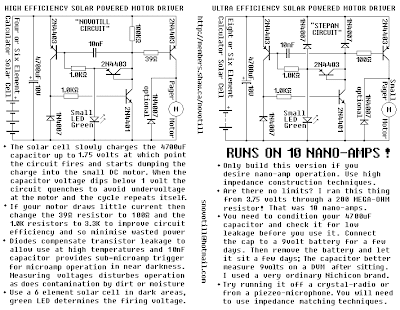
Simple Solar Engine Wiring diagram Schematic

 simple solar engine circuit diagram
 
Simple Solar Engine Circuit Diagram Small DC motor runs off of calculator solar cell in dim light. How do we achive 10nA operation? By using diodes in place of pull up resistors, and by isolating the DC load from the trigger schema via junction drops and the 10nF capacitor. If there is too much power comming from the solar cell then the motor might run too often or even continuously. You can avoid this by putting a 100K ohm resistor in series with the solar cell. 

 Simple Solar Engine Circuit Diagram

 simple solar engine circuit diagram

Read More..

Build a 4 Transistor FM Transmitter Wiring diagram Schematic

 4 Transistor FM Transmitter Circuit Diagram
 
 4 transistor fm transmitter circuit diagram

Build a  4 Transistor FM Transmitter Circuit Diagram. This 4 Transistor FM Transmitter Circuit Diagram provides an FM modulated signal with an output power of around 500mW. The input microphone pre-amp is built around a couple of 2N3904 transistors (Q1/Q2), and audio gain is limited by the 5k preset trim potentiometer. 

The oscillator is a colpitt stage, frequency of oscillation governed by the tank schema made from two 5pF ceramic capacitors and the L2 inductor. The output stage operates as a Class D amplifier, no direct bias is applied but the RF signal developed across the 3.9uH inductor is sufficient to drive this stage. The emitter resistor and 1k base resistor prevent instability and thermal runaway in this stage.
Read More..

Sunday, August 24, 2014

Stereo Amplifier Circuit with IC AN7142

 *note : Stereo Amplifier
Ive tried this Circuit Amplifier  and was resulting in very satisfactory . The sound that issued a very nice and smooth. Its just that there is little noise, but the noise will go away when a loud sound. And strange , sound effects can out by itself  and by simply adding tone control.
Minimum supply voltage is 5 volt , and maximum supply voltage is 18 volt . Maximum power output  2 X 10 watt with minimum impedance 4 Ohm.

See this schematic Circuit below :


This is schematic circuit and i design in simple circuit.
Click to view Enlarge
Read More..

Magnetometer

Magneto
Magnetometers are scientific instruments that are used to measure the direction and strength of magnetic fields in the location that the device is located. They are used both on Earth as well on space exploration missions due to the significant variations that are found in magnetic fields based on the nature of the environment, interaction of charged particles from the sun, and the magnetosphere.
Read more
Read More..

Kitchen Exhaustion Fan Controller

Exhaustion fan is a very important element in kitchens. Here may be a easy schema to manage kitchen fans by monitoring the ambient temperature. its engineered round the renowned precision integrated temperature sensor chip LM35 (IC1). remainder of the schema may be a non-traditional electromagnetic relay driver wired round the fashionable LED driver LM3914 (IC2). User will switch 3 presetted temperature levels employing a jumper/slide switch (JP1), that determines the warmth level to activate the relay and hence the electrical exhaustion fan wired through the relay contacts. It works off 12V DC power offer.

Kitchen Exhaustion Fan Controller  Circuit Schematic


Only one adjustment is needed during this kitchen Exhaustion fan controller schema. when construction, set jumper purpose in its 1st position, ie base terminal of T1 is connected to pin thirteen of IC2 and alter the preset P1 fastidiously in order that relay RL1 is energised when ambient temperature level reaches close to 29oC. but this is often not terribly vital as youll choose any threshold level by connecting the jumper points to alternative unused output pins of IC2 (here solely three outputs are used).
Read More..

Kicker WX10000 1 Warhorse

MSRP $9,999.99
With dimensions measuring 35 inches by 17 3/4 inches by 3 3/4 inches and a total weight of 66 pounds, the Warhorse is a monster of an amp. On the other hand, its about the same size as amps with much lower power output, say, around 3,000 watts. That raises the question of whether its efficient enough to actually make its claimed 10 kilowatts of power.

Before I get into it, lets look at what were working with. Kicker has rated this beast at 10,000 watts into a 2-ohm load, or 5,000 watts into a 4-ohm load. As far as the class, its not D, AB, or anything else you might be familiar with. In fact, the operation of this amp is so unique that Kicker has applied for a patent so they can classify it. Ill do my best to explain all that, but in the meantime study up on Class D operation and pulse width modulation as a reference point.

The amp has the usual features youd expect to find in a big subwoofer amp like 24dB/octave highpass and lowpass crossovers, 0 to 18dB of bass boost at 40Hz, and the absence of fuses. In addition, the Warhorse sports three ought-gauge power and three ought-gauge ground cable connectors, and two pairs of 8-gauge Anderson connectors for the speaker outputs. No, its not a stereo amp-strictly mono.

Eight indicator lights on the control panel reveal several conditions. PWR illuminates when the amp is on and working properly. NET shows that youre connected to the optional WXRC remote control, which offers expanded crossover slope selections in addition to being able to make adjustments from the driver seat. There are also LED indicators for over-voltage, under-voltage, overheated and short-circuit. The X-BNDW light tells you that you have set the lowpass crossover lower than the highpass crossover, while the Service light lets you know that you probably need to get the amp back to the Kicker service department or at least call the tech support line.

The unit looks like an oversized black briefcase with extruded fins running the length of each side. The top is an engraved black aluminum plate with a molded plastic hood over the entry for the power cables. The cast endcaps house the cooling fans and provide a very structural look to the whole unit. The power and ground-all six ought-gauge cables-come into the amp at almost the center of the top plate. All other connections and controls are hidden halfway along the nearside heat sink under a matching cover plate.

Circuitry
Looking under the cover, the first thing youll notice is the four planar transformers and the huge buss bars that run across the topside of the main circuit board. The transformers are about the size of your hand and resemble a stack of pancakes. The primary and secondary windings are stacked on top of each other rather than being several strands of wire intertwined. The turn ratio is 19 to 1, meaning there are literally 19 turns of flat wound copper for each secondary and one turn for each primary. The primary looks more like a big horseshoe-shaped PCB trace. Each planar transformer is rated at 5,000 watts for a total capacity of 20,000 watts.

The positive and negative power cables feed the transformers directly by way of the plated copper buss bars. The B+ power supply is stabilized by a total of 50 3,300F/105 C capacitors. That makes for a lot of instant juice on tap.
The entire backside of the heat sink is occupied by 64 MOSFETs, 16 for each of the four transformers. Normally, Id call these devices "switchers" to drive the transformers and create the positive and negative rails, but this is where we deviate substantially from every other amp. These MOSFETs do actually drive the transformers, but not at a steady rate to create a "reservoir" of output power. They actually drive the transformers directly to the speaker outputs in a pulse-width modulation fashion. This effectively eliminates the section of the amp that would normally be called the "output" section, and also eliminates the efficiency losses associated with output sections, whatever class they may be.

Lets look at the input section. The analog music signal from your head unit enters the amp by way of a pair of gold-plated RCA connectors, and goes pretty much straight to a Texas Instruments DSP chip. Theres plenty of support circuitry around the DSP. In fact, the input board is about 6 inches by 8 inches, but all of the processing goes on inside the chip. The gain, crossover, bass boost, and limiter controls are all single element potentiometers that feed reference signals to the DSP chip. In other words, they have no direct effect on the analog signal; they just tell the processor what you want it to do. Once the analog signal enters the DSP, theres no more analog signal until you get to the output filter at the speaker outputs. Because the crossovers and bass boost are handled in the digital domain, the curves are picture perfect and very precise.

Heres where things get even stranger. In a typical amp you have an input stage, a power supply stage, and an output stage where the first two stages work together to kick out the tunes. The power supply runs at a constant rate, creating a "reservoir" of power (called "rails") thats fed to the speakers through the output transistors as the input section commands. In the Warhorse, theres an input stage as usual, but the output and power supply stages are combined. Instead of creating a reservoir of power for the output stage to use, the DSP causes the power supply to actually create the output signal directly. Instead of running at a constant level, the power supplies are constantly going up and down (signal modulated) in response to the DSP to create the output voltage. There are no output transistors.

Thats the conceptual picture, pretty much devoid of the details. At this point you may be thinking, "Thats too easy" or "Why hasnt this been done before?" While the concept is easy, the execution requires a fairly powerful DSP, as well as a fairly powerful brain trust to program the DSP. On this scale (remember this amp puts out 10,000 watts), it also requires the planar transformers with specific coupling and power characteristics.

The DSP is in complete control of the transformers, running a constant pulse of 24kHz. That doesnt mean the transformers are creating a large 24kHz output signal, but thats the clock speed for the pulse-width modulation. When a signal comes into the DSP, it sends off/on pulses to the transformer switchers of the appropriate duration to create both the frequency and the amplitude of the output. In a pulse width modulation format the length of the pulse will correspond to the output voltage level, and in this amp the length of the pulses will be limited to 1/24,000 of a second. A maximum pulse (100 percent) will result in maximum power output, while a half-length pulse (50 percent) results in half power. At idle, theres zero current going through the transformers, but its still happening at 24kHz.

This is where the amp is like a Class D amp. If the transformer is completely accurate (not possible, by the way) the output will consist of really large squared waves. In reality, the transformer will round these square pulses considerably, plus theres an output filter consisting of a coil and capacitor(s) to finish converting the squared pulses to nice round sine waves. The output filter coils in the Warhorse actually look just like large transformers that would be used in the power supply of a big Class AB amp.

So you now have output signal to feed your speakers, and it should resemble the analog input signal that came into the DSP to start with. The DSP takes feedback from the speaker outputs and makes real-time adjustments to the pulses to create a more accurate reproduction of the original signal, only lots bigger.

There are two separate sets of speaker outputs on the Warhorse, but theyre not parallel. You have to use both of them and you have to use them on a dual voice coil speaker, one output to each coil of the speaker. One set handles the positive side of the wave and the other handles the negative side. The + and - labels on the amp correspond to the labels on the speakers voice coil terminals. At full power this amp is making around 141 volts between 20Hz and 200Hz. Household AC is 120 volts at 60Hz. If you fed the amp with a 60Hz signal, you could probably use it as a backup generator for your house, so dont mess around with the speaker outputs when this amp is on.

Performance
The amp tested as advertised in all respects. The frequency response is exactly 20Hz to 200Hz at the -3dB points, though we used +0/-1dB for the test results. The crossovers and bass boost are exact as well, which is a direct result of the signal being handled in the digital domain by the DSP chip. Power at 14.4-volt input exceeded 10 kilowatts by 350 watts-the equivalent of a decent subwoofer amp. While 10,000 watts is pretty impressive, the fact that the WX10000.1 can deliver it with almost 90 percent efficiency is amazing. Class AB amps hover around 50 percent, so this amp can deliver almost twice the output power for any given power input. You can feed two of these amps for the price of one.

There was no indication on the scope of any turn-on or turn-off noise. Who needs a 10,000-watt turn-on pop?

Slew rate and damping factor have been omitted from this test due to the way the amp works and the importance of such specs for an amp of this size. Testing was complicated by the fact that the DSP is instantly responding to the output feedback. The compensation by the DSP resulted in a negative ratio for the damping factor. The precision of the DSP also resulted in a very low slew rate at the output, which corresponded very closely to the actual slope of a wave at 200Hz. In other words, we were only able to measure what the DSP was causing the amp to do, rather than what it might be capable of.

Manual
The owners manual is a pretty comprehensive affair. In fact, I suggest you read the manual before purchasing the amp, just to make sure youre equal to the commitment. The manual is where you learn about having to build an electrical substation to feed the beast. Yes, Im exaggerating but seriously, Kicker recommends no less than eight batteries of 800cca plus two alternators putting out 200 amps each. Thats in addition to the battery and alternator just to run the vehicle. As well, you have to run ought-gauge cable everywhere to boot.

Besides the electrical requirements, and the structural mounting bracket, the manual shows several wiring configurations, and explains the controls clearly. The warranty is three months (consumer installed) or two years when installed by an authorized dealer.

Conclusion
Kicker has managed to break new ground here, and do it in a big way. The Warhorse is expensive, but its intended for use in decibel machines and show systems. The retail dollars-to-watts ratio is a pretty high 97 cents, but using this amp will reduce the overall cost of batteries and alternators due to its high efficiency. Check out the Kicker Warhorse van making appearances around the country if you want to experience what this kind of power is all about.


Test Results
Output power @ 1% THD, 50Hz, 14.4 volts
Mono @ 4 ohms 1 x 5,494 watts
Mono @ 2 ohms 1 x 10,350 watts
Output power @ 1% THD, 50Hz, 12.5 volts
Mono @ 4 ohms 1 x 4,050 watts
Mono @ 2 ohms 1 x 8,052 watts
Distortion at rated power, 50Hz, 14.4 volts 0.66% @ 2 ohms
Input sensitivity 165mV to 5.2 volts
Frequency response (+1dB) 25Hz - 170Hz
S/N ratio (A weighted, below clipping, min. gain) >82dB
Idle current 3.5 amps
Maximum current consumption, unclipped 801 amps @ 10,350 watts
Efficiency at one-third power, lowest impedance 88%
Efficiency at full power, 1%THD, lowest impedance 89.7%
Crossover slope 24dB/octave
Crossover range, lowpass 50Hz - 200Hz
Crossover range, highpass 20Hz - 60Hz
Low-frequency boost +18dB @ 40Hz
Dimensions 35"L x 17.75"W x 3.75"H
Weight 66.8 pounds
Read More..

Saturday, August 23, 2014

TDA7000 Single Chip FM Radio

This fm radio series fm radio receiver circuit that uses a single ic TDA.


Quite easy to make this fm radio circuit, where all functions can be done by IC TDA, so we only add to the technical components only. External components are intended to support so you can determine its own range of frequencies to be used. Actually if you want to have the radio equipment are satisfactory you can buy a radio market. Now this type of radio is very varied and the prices varying as well. To be sure with the money of 30 thousand you can get the fm radio with satisfactory quality. Because now the most sold radio is using digital functions, unlike the more dominant is the first transistor radio. But if you are a hobby with experimental electronics, not the rupiah value but which you consider the value of their knowledge.

For the working principle of this circuit does not really exist that must be addressed because all the functions already performed by the internal circuit is ic TDA. That if we do a surgical series is in the ic, the result will not be much different circuits fm radio receiver in general.

Component List:
1. IC TDA 7000
2. Resistor: 100 Kohm, 22 Kohm 100 Kohm and potensio
3. Capacitors: 39 pF, 37 pF, 220 nF, 22 nF, 10 nF, 180 pF, 150 pF, 100 nF, 330 pF, 220 pF, 3.3 nF, 330 pF, 3.3 pF, 220 nF, 1.8 nF, 1.8 nF, 25-50 pF
4. Inductors: 56 NH (2 pieces)
5. Loudspeaker
6. Antenna
Read More..

Stereo balance indicator


You can use this schema to modify your own amplifier.this shows the out put sound level.you can use this one for various things.


Notes.

* The schema can be assembled on a Vero board.
* Use 9V DC for powering the schema.
* Mount IC1 on a holder.
* C1 ,C2 and C3 must be rated at least 6V.

Read More..

Variable Zener Diode Wiring diagram Schematic

The schema behaves like a zener diode over a large range of voltages. The current passing through the voltage divider R1-R2 is substantially larger than the transistor base current and is in the region of 8 mA. The stabilizing voltage is adjustable over the range 5-45 V by changing the value of R2. The total current drawn by the schema is variable over the range 15 mA to 50 mA.This value is determined by the maximum dissipation of the zener diode. In the case of a 250 mW device, this is of the order of 50 mA.

Variable Zener Diode Circuit Diagram

Variable

Read More..