Friday, September 26, 2014

Over Current Mains Monitor Circuit Diagram

Bridge D4-D7 can only provide  the coil voltage for Ret when  the current through D1-D2 exceeds a certain level, because then series capacitor Ci passes the alternating mains 4 current.
Capacitor C1 may need to be dimensioned otherwise than shown to suit the sensitivity of the relay coil. This is readily effected by connecting  capacitors in parallel until the  coil voltage is high enough for  the relay to operate reliably.   

Over Current Monitor Circuit Diagram


Read More..

Tri Waveform Generator

The Tri-Waveform Generator can be used for a number of different uses. The one that I use it for is a signal generator to test circuits. The frequency range is 20 to 20khz. and can be adjusted by R1. The duty cycle or the time that the waveform is high and the time that the waveform is low can be adjusted by R4. The purpose of R2 and R3 are to clean up any distortion on the sine wave output. To do this you must hook up the sine wave output to and oscilloscope and adjust R2 & R3 to make the sine wave as accurate as possible.

Read More..

Power up down Sequencer

Whether you’re talking about a home cinema  or a computer system, it’s very often the case  that the various elements of the system have  to be turned on or off in a quite specific order,  or at least, automatically. Constructing this  sort of automation system is well within the  capability of any electronics enthusiast worthy of the name, but in this ‘all-digital’ age,  most of the circuits of this type to be found  in amateur electronics magazines or web-sites use a microcontroller. Even though that  is indeed a logical solution (in  more ways than one!), and you  might even say the easiest one, it  does pose problems for all those  people who don’t (yet) have the  facilities for programming these  types  of  IC.  So  we  decided  to  offer you now an approach that’s  very different, as it only uses a  simple, cheap, commonly-avail-able analogue integrated circuit,  which of course doesn’t have to  be programmed. Our project in  fact uses as it’s ‘brain’ an LM3914,  a familiar IC from National Semiconductors,  usually  used  for  driving  LED  VU  (volume  unit)  meters. 

Circuit diagram :
Power-up-down Sequencer Circuitw
Power-up/down Sequencer Circuit Diagram

Before taking a look at the circuit  for  our  project,  let ’s  just  remind ourselves that the IC has  one analogue input and ten out-puts intended for driving LEDs.  It can operate in ‘point’ mode,  where the LEDs light up in turn,  from first to last, depending on  the input voltage, but only one LED is lit at  any given time. Alternatively  it can operate  in ‘bar’ mode (this is the mode normally used  for VU meters), and in this case, the LEDs light  up one after the other, in such a way as to create a strip of light (bar) that is longer or  shorter according to the input voltage. This is  the mode selected for the LM3914 in the circuit described in some detail below. 

So as to be able to control the AC powered equipment  our  sequencer  is  intended  to manage, we are using solid-state relays — four, in our example, though you can reduce or increase this number, up to a maximum of ten. Since the input devices in solid-state relays are LEDs, they can be driven directly by the LM3914 outputs, since that’s exactly what they’re designed for. As only four relays  are available, these are spread across out-puts L2, L4, L6, and L8, but you can choose  any arrangement you like to suit the number  of relays you want to use. 

Resistor R7 connected to pin 7 of the LM3914  sets the current fed to the LEDs by the LM3914  outputs. Here, it’s been set to 20 mA, since  that is the value expected by the solid-state  relays chosen. The input voltage applied to  pin 5 of the LM3914 is none other than the  voltage present across capacitor C1 — and  this is where the circuit is ingenious. When  the switch is set to ‘on’, C1 charges slowly  through R5, and the LEDs of the solid-state  relays on the outputs light one after another  as this voltage increases; in this way, the units  being controlled are powered up in the order you’ve chosen. To power-down, all you have  to do is flip the switch so that C1 discharges  through  R5,  and  the  LEDs  go  out  in  the  reverse order to that in which they were lit,  in turn powering down the units connected to the solid-state relays. Easy, isn’t it? If you’re not happy with the sequence speed,  all you need do is increase or reduce the  value of R5 in order to alter the speed one  way or the other.
The circuit needs to be powered from a volt-age of around 9 to 12 V, which doesn’t even  need to be stabilized. A simple ‘plug-top’,  ‘wall wart’ or ‘battery eliminator’ unit will be  perfect, just as long as it is capable of supply-ing enough current to power all the LEDs. As  the LED current is set by R7 to 20 mA per LED,  it’ll be easy for you to work out the current  required, according to the number of solid-state relays you’re using. 

In our prototype the type S216S02 relays  from Sharp were used, mainly because they  proved readily available by mail order. They also have the advantage of being compact,  and their switching capacity of 16 A means  you can dispense with a heatsink if you’re  using them for a computer or home cinema  system, where the current drawn by the vari-ous units can be expected to remain under  1 A. These solid-state relays must be protected by a fuse, the rating of which needs to  be selected according to the current drawn  by the devices being powered. 

Also note the presence across the relay terminals of a VDR, also known as a GeMOV or  SiOV, intended to protect them from any spurious voltage spikes. You can use any type  that ’s intended for operation on 250 VAC  without any problem. The values of fuses F1  to F4 are of course going to depend on the  load being protected. 

Construction of the circuit shouldn’t present any particular difficulty, but as the solid-state relays are connected directly to AC  power, it is essential to install it in a fully-insulated case; the case can also be used to  mount the power outlet sockets controlled  by the circuit. Note that sockets are female  components.
Let’s just end this description with the sole  restriction imposed by our circuit — but it’s  very easy to comply with, given the intended  use. In order to remain triggered, the solid-state relays must carry a minimum holding  current, which is 50 mA in the case of the  devices we’ve selected. In practical terms,  this just means that each of the devices powered by our sequencer must draw at least  50 mA, or in other words roughly 12 VA at  230 VAC, or 25 VA at 120 VAC.

Author :Christian Tavernier
Read More..

Ultra Simple Microphone Preamplifier

This little project came about as a result of a design job for a client. One of the items needed was a mic preamp, and the project didnt warrant a design such as the P66 preamp, since it is intended for basic PA only. Since mic preamps are needed by people for all manner of projects, this little board may be just whats needed for interfacing a balanced microphone with PC sound cards or other gear. Unlike most of my boards, this one is double-sided. I normally avoid double-sided PCBs for projects because rework by those inexperienced in working with them will almost certainly damage the board beyond repair.
I consider this not to be an issue with this preamp, because it is so simple. It is extremely difficult to make a mistake because of the simplicity. As you can see, the board uses a PCB mounted XLR connector and pot, so is a complete mic preamp, ready to go. Feel free to ignore the terminals marked SW1 (centred between the two electrolytic supply caps), as they are specific to my clients needs and are not useful for most applications. The original use was to use them for a push-button switch that activated an audio switch via a PIC micro-controller. They are not shown on the schematic.
 P12-pic

The DC, GND and output terminals may be hard wired to the board, you may use PCB pins or a 10-way IDC (Insulation Displacement Connector) and ribbon cable. Power can be anything between +/-9V and +/-18V with an NE5532 opamp. The mic input is electronically balanced, and noise is quite low if you use the suggested opamp. Gain range is from about 12dB to 37dB as shown. It can be increased by reducing the value of R6, but this should not be necessary. Because anti-log pots are not available, the gain control is not especially linear, but unfortunately in this respect there is almost no alternative and the same problem occurs with all mic preamps using a similar variable gain control system.
P12-f1

The circuit is quite conventional, and if 1% metal film resistors are used throughout it will have at least 40dB of common mode rejection with worst-case values. The input capacitors give a low frequency rolloff of -3dB at about 104Hz. If better low frequency response is required, these caps may be increased to 4.7uF or 10uF bipolar electrolytics. These will give response to well below 10Hz if you think youll ever need to go that low. The project PCB measures 77 x 24mm, and the mounting centers for the pot and XLR connector are spaced at 57mm. If preferred, a traditional chassis mounted female XLR can be used, and wired to the board with heavy tinned copper wire. The PCB pads for the connector are in the correct order for a female chassis mount socket mounted with the "Push" tab at the top.
source: www.sound.westhost.com
Read More..

Voltage Tester for Model Batteries

With a suitable load, the terminal voltage of a NiCd or lithium-ion battery is proportional to the amount of stored energy. This relationship, which is linear over a wide range, can be used to build a simple battery capacity meter. 

Circuit Image :
 Voltage Tester for Model Batteries Image
Voltage Tester for Model Batteries Circuit Image 

This model battery tester has two functions: it provides a load for the battery, and at the same time it measures the terminal voltage. In addition, both functions can be switched on or off via a model remote-control receiver, to avoid draining the battery when it is not necessary to make a measurement. The load network, which consists of a BC517 Darlington transistor (T2) and load resistor R11 (15 Ω /5 W), is readily evident. When the load is active, the base of T1 lies practically at ground level. Consequently, T1 conducts and allows one of the LEDs to be illuminated. 

Circuit Diagram :
Voltage Tester for Model Batteries-Circuit Diagram
Voltage Tester for Model Batteries Circuit Diagram

The thoroughly familiar voltmeter circuit, which is based on the LM3914 LED driver, determines which LED is lit. The values of R6 and R7 depend on the type and number of cells in the battery. The objective here is not to measure the entire voltage range from 0 V, but rather to display the portion of the range between the fully charged voltage and the fully discharged voltage. Since a total of ten LEDs are used, the display is very precise. For a NiCd battery with four cells, the scale runs from 4.8 V to 5.5 V when R6 = R7 = 2 kΩ. The measurement scale for a lithium-ion battery with two cells ranges from 7.2 V to 8.0 V if R6 = 2 kΩ and R7 = 1 kΩ. 

For remote-control operation, both jumpers should be placed in the upper position (between pin 1 and the middle pin). In this configuration, either a positive or negative signal edge will start the measurement process. A positive edge triggers IC1a, whose output goes High and triggers IC1b. A negative edge has no effect on IC1a, but it triggers IC1b directly. In any case, the load will be activated for the duration of the pulse from monostable IC1b. Use P12 to set the pulse width of IC1a to an adequate value, taking care that it is shorter than the pulse width of IC1b. 

If the voltage tester is fitted into a remote-controlled model, you can replace the jumpers with simple wire bridges. However, if you want to use it for other purposes, such as measuring the amount of charge left in a video camera battery, it is recommended to connect double-throw push-button switches in place of JP1 and JP2. The normally closed contact corresponds to the upper jumper position,while the normally open contact corresponds to the lower position.

Parts :
Resistors:
R1,R2 = 47kΩ
R3 = 100kΩ
R4 = 500kΩ
R5 = 1kΩ
R6,R7 = see text (1% resistors!)
R8 = 1kΩ5
R9 = 1kΩ2
R10 = 330Ω
R11 = 15Ω 5W
R12 = 15kΩ
P1 = 100kΩ preset
Capacitors:
C1 = 10nF
C2 = 100nF
Semiconductors:
D1-D10 = LED, red, high effi-ciency
T1 = BC557
T2 = BC517
IC1 = 74HC123
IC2 = LM3914AN
Miscellaneous:
PC1,PC2,PC3 = solder pin
JP1,JP2 = jumper or pushbutton

PCB Layout :
B. PCB Laout
Voltage Tester for Model Batteries PCB Layout


Copyright : Elektor
Read More..

FTDI Bitbang IR Remote Transmitter Receiver

I use my computer every single minute, I do my work at home and I need to finish lots of paperwork. My computer helps me in almost everything I do. I make sure that my pc is able to do multitasking and functioning well. Just like our body, it should be fit to do all the workload that must be finished within the day.

FTDI Bitbang IR Remote
To come up with another task that a pc can add to its functions, an IR remote was created through an FTDI that receives and transmits data other than the Universal Serial Bus. This is definitely a big help that my pc can easily cope up with simultaneously.

FTDI Bitbang IR Remote
Read More..

Make Your Iphone Battery Last Longer

I’ve owned a Iphone for a while now, it’s an amazing phone, the best I have ever used so far. But when I first started using it, my only concern was that the battery didn’t last as much as I expected. After two days, it was gone, and when I needed it, the phone just didn’t turn ON. I used to let the wireless on almost all the time and downloading many new apps. Now that I have some more experience on how my little gadget works, I will try to share some ideas on how you can optimize your iphone’s battery life and have a better iExperience.

iphone

  • Wireless connectivity will drawn your battery even if you are not using it. Keeping it on, it will always try to connect to some open hot spot, try to check your emails and much more. So a good idea is to turn it on when using, and after, turn it off.
  • Bluetooth have a similar battery usage as Wi-Fi, so there’s not much reason to leave it on if you are not using it (I believe that the most common usage for bluetooth today is the headsets and car kits).
  • Auto-Brightness is a interesting thing apple made to make the battery last longer. It uses iphone’s camera to adjust brightness based on the lighting conditions outside, so it will automatically set, for example, to make it less bright when you are on a dark place. Great feature!
  • Music EQ will have a significant battery usage if you listen to your songs for many hours everyday, as it uses more processing power. So if you want to charge less your iphone, it is another thing you may consider turning it off.
  • Heat can be a problem to your iphone, as it is a very bad thing to lithium-ion batteries, making them harder to charge and destroying it due the intense ionization. So remember to never let your phone in a hot place such as inside a car or in direct sunlight. If you are using some kind of carrying case, you need to be even more careful about this, and remember to take it off when charging your mobile, as it gets warm when charging.
  • Keep it charging! After putting your phone to charge, leave it there for some hours more after it says it’s full. It will make your phone battery last much more, you will be surprised! After done that, my iphone battery lasted more then a week, way more if you compare to the 2-3 days when I was disconnecting if from the dock just after it says its full.
  • Background Programs! This is important, new iphones, such as Iphone4 allows you to run multiple apps on the background, but this will drain your battery fast if you forget to close them. To do this, double click on the round button and it will show all the apps currently running, keep clicking in one of the apps and a red “X” will apear, then you can close all apps.
  • What else do you do to make your iphone battery last longer?


    Source by : link
    Read More..

    Simple Code Lock Circuit Diagram

    The above cycle is therefore repeated only when S7 at the Q1 output is pressed in time. When all keys have been pressed in time and in the correct order, Q7 goes 5 high for about 4 seconds to enable driving the unlock circuitry, e.g. a relay driver for an j automatic door opener.

     At the i heart of the circuit is the Type 4022 octal counter. In the non- active state, Cz is charged via R5, so that the reset (R) input of the counter is kept logic high.
     This causes output Qc to be actuated, while all other outputs are logic low. When S1 is pressed, T1 is switched on via debouncing network Rz—C1, and IC1 receives a clock pulse. Also, Cz is discharged via R4-D1, ending the reset state of the counter and enabling it to I advance.
    This code lock provides a high degree of security whilst being i a very simple design.
    The time required for Rs to recharge Cz, i.e., to reset the counter, is the maximum time that can lapse before the next key is pressed.
    The 5 code for the lock shown in the T circuit diagram is 1704570: this is but an example, however, and i the combination code is readily Y altered by swapping connections between the counter out- puts and the switches.
    When the Zdigit code is considered too simple to crack, the 4022 can be replaced by a 4017,   which makes it possible to add two keys.
    This means that the number of combinations is 109 instead of 107. The quiescent current consumption of the code lock ` negligible at 0.5 JA, so that the operation is feasible. The circuit works well from any supply between 6 and 15V 

    Simple Code Lock Circuit Diagram


    Read More..

    IC 741 Opamp Parameters Explained

    It is important to know the typical parameters of the op-amp before trying it in a new application so as to get the best results.
    Some important parameters and their significance are mentioned below: Open loop voltage gain Ao: This is the basic voltage gain of the internal circuitry as a whole, and may be expressed as a multiple or in decibels. A typical value of A0 for 741 is 1.00,000 or 100 dB.


    Input impedance Zm: This is a measure of the impedance, looking into the input terminals of the op-amp, and is expressed in terms of resistance. A typical value of Zm for 741 is 1 megohm

    Output imped¢mce—Zo: Tliis is a measure ot the impe- dance offered by the output terminals of the op-amp. It is also expressed in terms of resistance. A typical value of Zo for 741 is 150 ohms.

    Input bias current-Ir: Op-amps utilising bipolar transistor input stages draw a small bias current from the input terminals. A typical value of Ib for 741 is 200 nA (200x 10^-9 amperes).

    Input voltage range- Vi(max): This is the maximum value of input voltage that can be connected to the input without causing any damage. It is usually lower than the operating supply voltages. A typical value of Vi(max) for 741 is +/-13V (for the supply voltages +/-15V).

    Output voltage range- Vo (max): If the op-amp is over- driven, its output will saturate and be limited by the operating supply voltages. So, Vo(max) is usually specified as being one or two volts less than Vs. A typical value of Vo(max) 741 is +/- 14V (for the supply voltages +/-15V).

    Supply voltage range- Vs: Op—amps are usually operated from dual supplies that are anywhere between their minimum and maximum limits. lf the supply voltages are very » high, the op-amp may get damaged. lf they are very low, the op-amp may not work satisfactorily. Typical supply limits for 741 are +/- 6V to +/- 18V.

    Differential input offset voltage- Vio: Due to slight imbalances within their input circuitry and due to high gain of the op-amp, it is observed that the output does not register zero voltage even when both inputs are grounded. This small imbalance voltage appearing in the input, which may even cause the output to swing to saturation, is known as the differential input offset voltage. A typical value of Vio for 741 is 2 mV. lt is often required in some particular. op-amp applications to nullify this offset voltage by using external offset nulling circuit, as shown in Fig. (m).

    Common mode rejection ratio-CMRR: In an ideal op- amp, if an identical signal is applied to both the inputs, the resultant output is zero. However, in practical op-amps, common mode signals do not entirely cancel out and produce a small signal at the output terminals. The ability of the op-amp to reject common mode signals is usually expressed in terms of common mode rejection ratio. CMMR is the ramp of the op-amp gain with differential signals to the· op-—-amp gain with common mode signals. CMRR value for 741 is typically 90 dB.

    Transition frequency-fr: This is the frequency at which the gain of the op-amp falls to unity, Though an op-amp has a very high gain at low frequencies, inthe interest of stability its open loop frequency response is tailored so that the gain falls off as the frequency rises. The gain falls to unity at a transition frequency known as fr. The value of fr for 741 is 1 — MHZ.


    Read More..

    Thursday, September 25, 2014

    Voltage Controlled Oscillator Circuit

    A simple voltage controlled oscillator circuit which produces both triangular and square wave outputs is shown.
    Then the output of the Schmitt trigger is high, the clamp transistor TR; is conducting and the input current passing through R2 is shunted to ground. The current passing through R 1 causes a falling ramp to be formed. When the Schmitt circuit changes state, its output switches TR; to the nonconducting state. The current flowing through R2 can be made twice that flowing through Fl; (R2 = R;/2) so that the rising part of the ramp has a similar slope to the negative part.  The greater the value of the control voltage, the greater the frequency of oscillation. However,  the voltage must exceed the constant input voltage (V,) or the circuit will fail to oscillate. 


    Read More..

    Simple Neon Lamp Tester Circuit

    1. This tester can also be used to check IF transformers used in AC mains operated radio receiver.
    2. Though this tester is not very accurate, it can give a reasonably good indication about the condition of the components being tested.
    3. Neon lamps are ideal indicators for simple testers to check large resistances of leaky capacitors and mains lF transformers.
    4. For accuracy, the component being tested should not have any shunting resistance. lf a shunting resistance is present, disconnect one end of it before testing.
    5. Such a defective component cannot be easily tested with simple test equipment.
    6. The tester circuit uses a relaxation oscillator, the frequency of which is determined by capacitor Cl and the external resistance (leakage resistance of the component under test) between the probes.
    7. Two flashes per second on neon lamp indicates 200 megohm leakage resistance, four flashes l00 megohm, eight flashes 50 megohm, and so on.
    8. Moreover, as it tests capacitors at a fairly high voltage—closer to that of the operating voltage-it offers an advantage over a VTVM which is operated at a low voltage and gives inconclusive results.
    9. Being high-voltage, low-current devices, the neon lamps are very sensitive.
    10. The grid of an IF amplifier usually has a high AC impedance and its primary is operated at a high voltage.
    11. A small leak in the lFl` can cause considerable trouble. 

    Read More..

    Simplest Automatic Ni Cd Battery Charger Circuit Using IC 555

    The 555 timer can conveniently function as the heart of an automatic Ni-Cd battery charger, the circuit is intended to maintain a full charge on a standby battery supply for an instrument that is always connected to the mains, whether in use or not. lt can also be used for the charger unit for pocket calculators, etc.
    The circuit uses the timer’s two on-chip comparators, the flip flop and driver amplifier. A zener provides a reference voltage somewhere near the battery voltage with an allowance for adjustment.

    The two potential divider networks supply the comparators with adjustable voltages, one for LOW (switch on) and the other for HlGH (switch off). When on, the output gives a maximum of 10V and when off gives GV, the maximum current is 150mA which is limited by the ·47 ohms and protected by the diode.  The circuit is calibrated by substituting a variable voltage supply for the Ni-Cd batteries., The HIGH adjustment is set first so that the output switches off at the maximum battery  voltage and then the LOW is set for minimum battery voltage. It is simplest to leave the output disconnected from the resistor until after the setting up procedure. 


    Read More..

    Simple UJT Timer Circuit

    ln operation, the peak point requirement of UJT O1 is reduced to about } 1/1000 · of its normal requirement by pulsing its upper base with a volt negative pulse derived from the free running oscillator UJT I O2
    This regular pulse momentarily reduces the peak point voltage of O1 1 and thus allows the peak point current to be supplied from C1 rather than F1‘1,` as it would be with the more conventional circuits of this type. The pulse rate of oscillator O2 is not very critical but it should have a period that is less than one fiftieth of the overall time delay.

    Simple UJT Timer Circuit


    Read More..

    Wednesday, September 24, 2014

    Simple Neon Tube Flasher Circuit

    Flashing neon globes have use in many applications, however their relatively high working voltage precludes their general use where a mains supply is not available.
    This simple neon tube flasher circuit enables neon tubes or bulbs to be operated from a low voltage dc supply. The voltage required to ignite the neon tube is obtained by using an ordinary filament transformer (240-6.3Vl in reverse. Battery drain is quite low  being in the region of 1 to 2 milliamps for a nine volt battery. O1 is a unijunction transistor and operates as a relaxation oscillator. its frequency of operation is determined by R2-C1.  The pulses from Q1 are directed to O2 which in tum drives O3 into saturation. The sharp rise in current through the 6.3V winding of the transformer as 03 goes into saturation induces a high voltage in the secondary winding causing the neon to flash.  The diode D1 protects the transistor from high voltage spikes generated when switching currents in the transformer. 


    Read More..

    High Voltage Generator Circuit Diagram

    This is a short  High Voltage Generator Circuit Diagram of a high voltage generator and can be mounted in a small space and powered by rechargeable or simple batteries, the circuit generates a voltage low current but a high turn-on of about 200 to 400 V harmless to humans, of course, but is able to give a pretty nasty shock. 

     High Voltage Generator Circuit Diagram

     High Voltage Generator Circuit Diagram


    Here is a project that could be useful this summer on the beach, to prevent anyone touching your things left on your beach towel while you was swimming, you can equally well use it in the office or workshop when you return to work. It operates as a low frequency oscillator, which makes it possible to convert the battery voltage into a DC voltage alternating current that can be enhanced through the transformer. 

    Using a transformer with center tap as herein makes possible the construction of a Hartley oscillator transistor T1 around The output voltage can be used directly through R2 and R3 current limiting resistors, which should not in any circumstances be omitted or modified, they are what make the circuit have security. You will then get about 200 V peak-to-peak, which is already quite unpleasant to the touch. 

    But you can also use a voltage doubler, shown at the bottom right of the figure, which will produce about 300 V, even more unpleasant to the touch. Here too, of course, the resistance, you know how R4 and R5, should always be present. It can be used in small electric fences, chase away animals, etc.
    Read More..

    DC Voltage Doubler using the 74HC132 Circuit Diagram

    This circuit is a cheap way is a simple DC voltage doubler, which requires a few components and will generate a voltage 10Vdc from a 5Vdc power supply that can be output from the PC USB. The oscillator should be constructed from a non-functional door IC 74HC132 then requires more than two components are R1 and C3. The most important parameters of the voltage doubler circuit are given in the table schema.

    Note 
    That due to the tolerances of the data IC may have a few differences.


    DC Voltage Doubler using the 74HC132 Circuit Diagram


    Read More..

    Simple FAN 7710 Ballast Control

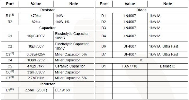
    Using the FAN 7710 Ballast Control IC for Compact Fluorescent Lamps developed using Fairchild’s unique highvoltage process and system-in-package (SiP) concept can be designed a very simple low cost fluorescent lamp driver electronic project .The FAN7710 ballast control controls internal high-voltage stress and delivers 20W to the lamp at 320VDC voltage.

    FAN7710 ballast control incorporates a preheating /ignition function, controlled by an user-selected external capacitor, to increase lamp life. The FAN7710 detects switch operation from after ignition-mode through an internal active Zero-Voltage Switching (ZVS) control circuit.


    The AC line input voltage (230 VAC 50 Hz) is rectified to provide a bus voltage of approximately 320 volts DC. Startup resistor R1 supplies initial power to the FAN7710 IC.The IC begins to oscillate and the charge pump circuit consisting of C2, D2 and D7 supplies the current to the VDD pin, which gets regulated through the internal 15-V shunt regulator.

    FAN7710 Ballast Control
    Read More..

    Animal Friendiy Mousetrap

    This mousetrap is built around a PlC12F683 and uses an infrared transmissive optical sensor that is modulated at a frequency of 38 kHz, so that it isnt affected by the ambient light. The modulation is carried out by the PlC, which generates a 38 kHz signal at port GP2, which is connected to the lR LED. The lR receiver is a type that is usually found for use with remote controls. lt reacts only to 38 kHz signals. lt reports the presence of an lR signal to the PIC via port GP1.
    When the lR lightbeam is broken the PIC turns of the relay via port GP4 and FET T1 , which: causes the door of the mousetrap to close. The transmissive optical sensor is housed inside a small wooden box. A small amount of food is placed inside this box.
    Circuit diagram :
    Animal Friendiy Mousetrap-Circuit diagram
    Animal Friendiy Mousetrap Circuit Diagram
    When a mouse walks through the light beam on its way to the food it causes the door to shut behind it and an LED starts flashing. The door is normally kept open by the coil of a relay that has been taken apart. When the coil is no longer powered the tin door is pushed shut by means of a spring. A piece of glass or transparent plastic should be put on top of the box, so that the mouse doesnt have to enter a dark space. When a mouse has been caught it can be let free again somewhere outside, some distance away from the house. 

    The reset button has to be pressed to ready the trap for its next victim. The author has managed to catch a few dozen mice with this device. The program is written in PICBASIC Pro and can be freely downloaded from the Elektor website, it is found in archive file # 100308-11.zip.
    Read More..

    Soft Start For Switching Power Supply

    Switching power supply whose output voltage is appreciably lower than its input voltage has an interesting property: the current drawn by it is smaller than its output current. However, the input power (UI) is, of course, greater than the output power. There is another aspect that needs to be watched: when the input voltage at switch-on is too low, the regulator will tend to draw the full current. When the supply cannot cope with this, it fails or the fuse blows. It is, therefore, advisable to disable the regulator at switch-on (via the on/off input). until the relevant capacitor has been charged. When the regulator then starts to draw current, the charging current has already dropped to a level which does not overload the voltage source.

    Circuit diagram:Soft Start Circuit Diagram For Switching Power Supply
    Soft Start Circuit For Switching Power Supply

    The circuit in the diagram provides an output voltage of 5 V and is supplied by a 24 V source. The regulator need not be disabled until the capacitor is fully charged: when the potential across the capacitor has reached a level of half or more of the input voltage, all is well. This is why the zener diode in the diagram is rated at 15 V. Many regulators produced by National Semiconductor have an integral on/off switch, and this is used in the present circuit. The input is intended for TTL signals, and usually consists of a transistor whose base is accessible externally. This means that a higher switching voltage may be applied via a series resistor: the value of this in the present circuit is 22 kΩ. When the voltage across the capacitor reaches a level of about 17 V, transistor T1 comes on, whereupon the regulator is enabled.
     
     
    Source: National Semiconductors
    Read More..

    Emergency Light using Phone Line Circuit Diagram

    This is a circuit for emergency lighting with LEDs that uses electricity from the telephone line. Generally the phone line has a DC voltage 48V and somewhere around 20 mA, and when the phone rings, the voltage rises to 96V AC. This works in a way that the phone line will not be busy while the LEDs are turned on and when you pick up the phone, the light goes off and lets you use your phone normally.

     Emergency Light using Phone Line Circuit Diagram

    Emergency Light using Phone Line Circuit Diagram

    Read More..

    How to Reuse Old Cell Battery for LED lighting

    Normally cell batteries have a shelf life of 2 to 5 years under normal use. After that time we have to replace them. Nowadays there replacement batteries which are cheap, but these batteries last for much less cost only months. An easy solution is to use batteries in a circuit that requires less current, we can use them for lighting LEDs.

     How to Reuse Old Cell Battery for LED lighting 

    How to Reuse Old Cell Battery for LED lighting

    Read More..

    Simple Fluorescent Without Transformer Circuit Diagram

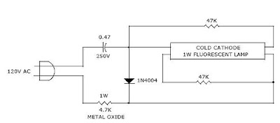
    This circuit caught my attention by using cold cathode fluorescent lamp and especially do not use any processor or oscillator. The circuit is powered by the AC mains of 110/127 and apparently the lighting power decrease significantly, but it is interesting to test.

    This simple circuit Fluorescent Lamp without transformer, operates from 120V AC, uses cold cathode fluorescent lamp and uses an RC circuit to limit the current. Caution! This assembly can be dangerous and cause shocks! We are not responsible for damages and malpractice in the assembly.

    Simple Fluorescent Without Transformer Circuit Diagram

    Simple Fluorescent Without Transformer Circuit Diagram

    Read More..

    PC Heat Monitor

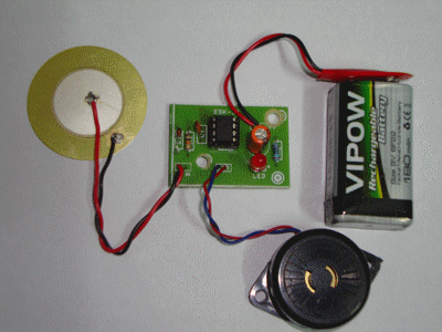
    The PC processor generates very high temperature during its operation which is dissipated by the large heat sink placed above the processor. If the heat sink assembly is not tight with the processor or the cooling fan is not working, PC enters into the Thermal shutdown mode and will not boot up. If the PC is not entering into thermal shutdown, the high temperature can destroy the processor. This simple circuit can be placed inside the PC to monitor the temperature near the processor. It gives warning beeps when the temperature near the heat sink increases abnormally. This helps to shutdown the PC immediately before it enters into Thermal shutdown.


    Circuit Project: PC Heat Monitor Circuit 
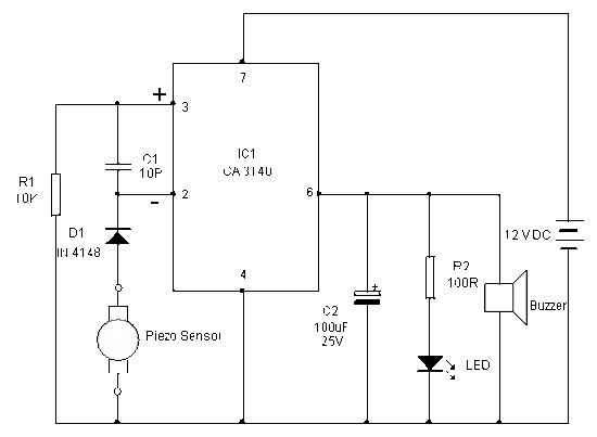
    The circuit uses a Piezo element (one used in Buzzer) as the heat sensor. The piezo crystals reorient when subjected to heat or mechanical stress and generates about one volt through the Direct piezoelectric property. IC1 is designed as a voltage sensor with both the inputs tied through the capacitor C1.The non inverting input is connected to the ground through R1 to keep the output low in the standby state. The inputs of IC1 are very sensitive and even a minute change in voltage level will change the output state.
    Circuit Project: PC Heat Monitor Circuit
    In the standby mode, both the inputs of IC1 are balanced so that output remains low. When the Piezo element accepts heat, it generates a minute voltage which will upset the input balance and output swings high. This triggers LED and Buzzer. Capacitor C2 gives a short lag before the buzzer beeps to avoid false triggering. Warning beep continues till the piezo element cools.
    Note: Enclose the circuit inside the PC with the piezo element close to the heat sink of the processor. Adjust the distance between the piezo element and heat sink so as to keep the circuit standby in the normal condition. The piezo element can sense a 10 degree rise in temperature from a distance of 5 cms. Power to the circuit can be tapped from the 12 volt line of SMPS.


    Sourced by Dr. Mohn kumar
    Read More..

    Low Dropout Adjustable Breadboard Power Supply

    This project details the design of a very low dropout adjustable power supply. A good power supply is essential to electronic projects. While there are many existing designs for adjustable power supplies, this one makes improvements that make it more useful for hobby designs

    Very Low Dropout Adjustable Breadboard Power SupplyMIC2941 regulator has guaranteed 1.25A output
    Low dropout, only 40mV - 400mV compared to 1.25V - 2.0V for LM317. This means you can use a wider range of output voltages including generating 3.3V from as low as 3.7V (such as 3 AAs or a lithium ion battery)!
    Short circuit and overheating protection
    Input diode to protect circuitry from negative voltages or AC power supplies.
    2.1mm DC jack and terminal connector for voltage inputs
    Two indicator LEDs for high and low voltages
    Output selection switch to select from 3.3v, 5v and Adjustable
    On-board potentiometer for adjusting voltage from 1.25V up to within 0.5V of the input voltage. (20V max)
    On/Off switch for entire board
    Very Low Dropout Adjustable Breadboard Power Supply Circuit Diagram
    Read More..

    Hot 2 Watt Audio Amplifier

    This amplifier was designed to be self-contained in a small loudspeaker box. It can be feed by Walkman, Mini-Disc, iPod and CD players, computers and similar devices fitted with line or headphone output. Of course, in most cases you will have to make two boxes to obtain stereo.

    Circuit Diagram:


    Parts:

    P1 = 10K
    R1 = 33K
    R2 = 33K
    R3 = 33R
    R4 = 15K
    R5 = 1K
    R6 = 1K
    R7 = 680R
    R8 = 120R-1/2W
    R9 = 100R-1/2W Trimmer Cermet
    C1 = 10µF-63V
    C2 = 10µF-63V
    C3 = 100µF-25V
    C4 = 470µF-25V
    C5 = 47pF-63V
    C7 = 470µF-25V
    C6 = 220nF-63V
    C8 = 1000µF-25V
    D1 = 1N4148
    Q1 = BC560C
    Q2 = BC337
    Q3 = TIP31A
    Q4 = TIP32A
    SW1 = SPST switch
    SPKR = 3-5 Watt Loudspeaker

    Circuit Operation:

    The circuit was deliberately designed using no ICs and in a rather old-fashioned manner in order to obtain good harmonic distortion behavior and to avoid hard to find components. The amplifier(s) can be conveniently supplied by a 12V wall plug-in adapter. Closing SW1 a bass-boost is provided but, at the same time, volume control must be increased to compensate for power loss at higher frequencies. In use, R9 should be carefully adjusted to provide minimal audible signal cross-over distortion consistent with minimal measured quiescent current consumption; a good compromise is to set the quiescent current at about 10-15 mA. To measure this current, wire a DC current meter temporarily in series with the collector of Q3.
    Read More..

    Simple Power inverter is Bidirectional Circuit Diagram

    If you want to swap charge in either direction between unevenly loaded positive and negative battery buses, you need an inverting dc transformer. One implementation is the symmetrical fly back converter shown in Figure 1 . The circuit can generate a negative output from a positive supply or a positive output from a negative supply.

    When the circuit starts up, the substrate diode of the output FET bootstraps the output voltage to the point where synchronous switching takes over. When the gate-switching signal is symmetrical, the output voltage is approximately -95% of the input voltage, and the efficiency is greater than 80%. You can obtain voltage step-up or step-down by adjusting the switching ratio.

    Power inverter is Bidirectional Schematic


    When I used the circuit between two 4V lead-acid batteries, a comparator adjusted the switch ratio to drive charge in the desired direction. The circuit automatically replaces charge drained from one battery to the other. In a short-battery-life application, the 2.5-mA standby current from each battery may be negligible. Using lower-gate-capacitance, FETs can reduce losses. Alternatively, you can add gates to the drive circuit to turn off both FETs whenever the battery voltages balance.

    The minimum input voltage is a function of the gate thresholds of the FETs. The ±9V rating of the CMOS 555 timer sets the maximum voltage. My prototype supplies approximately 100 mA Link
    Read More..

    Transformerless Power Supply

    This circuit will supply up to about 20ma at 12 volts. It uses capacitive reactance instead of resistance; and it doesnt generate very much heat.The circuit draws about 30ma AC. Always use a fuse and/or a fusible resistor to be on the safe side. The values given are only a guide. There should be more than enough power available for timers, light operated switches, temperature controllers etc, provided that you use an optical isolator as your circuits output device. (E.g. MOC 3010/3020) If a relay is unavoidable, use one with a mains voltage coil and switch the coil using the optical isolator.C1 should be of the suppressor type; made to be connected directly across the incoming Mains Supply.

    They are generally covered with the logos of several different Safety Standards Authorities. If you need more current, use a larger value capacitor; or put two in parallel; but be careful of what you are doing to the Watts. The low voltage AC is supplied by ZD1 and ZD2. The bridge rectifier can be any of the small Round, In-line, or DIL types; or you could use four separate diodes. If you want to, you can replace R2 and ZD3 with a 78 Series regulator. The full sized ones will work; but if space is tight, there are some small 100ma versions available in TO 92 type cases. They look like a BC 547. It is also worth noting that many small circuits will work with an unregulated supply.

    Circuit diagram:Transformerless Power Supply Circuit Diagram
    Transformerless Power Supply Circuit Diagram

    You can, of course, alter any or all of the Zenner diodes in order to produce a different output voltage. As for the mains voltage, the suggestion regarding the 110v version is just that, a suggestion. I havent built it, so be prepared to experiment a little. I get a lot of emails asking if this power supply can be modified to provide currents of anything up to 50 amps. It cannot. The circuit was designed to provide a cheap compact power supply for Cmos logic circuits that require only a few milliamps. The logic circuits were then used to control mains equipment (fans, lights, heaters etc.) through an optically isolated triac.

    If more than 20mA is required it is possible to increase C1 to 0.68uF or 1uF and thus obtain a current of up to about 40mA. But suppressor type capacitors are relatively big and more expensive than regular capacitors; and increasing the current means that higher wattage resistors and zener diodes are required. If you try to produce more than about 40mA the circuit will no longer be cheap and compact, and it simply makes more sense to use a transformer. The Transformerless Power Supply Support Material provides a complete circuit description including all the calculations.

    Web-masters Note:
    I have had several requests for a power supply project without using a power supply. This can save the expense of buying a transformer, but presents potentially lethal voltages at the output terminals. Under no circumstances should a beginner attempt to build such a project.

    Important Notice:
    Electric Shock Hazard. In the UK,the neutral wire is connected to earth at the power station. If you touch the "Live" wire, then depending on how well earthed you are, you form a conductive path between Live and Neutral. DO NOT TOUCH the output of this power supply. Whilst the output of this circuit sits innocently at 12V with respect to (wrt) the other terminal, it is also 12V above earth potential. Should a component fail then either terminal will become a potential shock hazard.
    MAINS ELECTRICITY IS VERY DANGEROUS.

    If you are not experienced in dealing with it, then leave this project alone. Although Mains equipment can itself consume a lot of current, the circuits we build to control it, usually only require a few milliamps. Yet the low voltage power supply is frequently the largest part of the construction and a sizeable portion of the cost.


    Author: Ron J - Copyright: Zen
    Read More..

    AC Mains Voltage Stabilizer Circuit

    It will be easier to understand the operation of the circuit if we separate the under and over-voltage protection circuitry comprising transistors T1, T2 and associated components from the rest of the regulator circuit. Diode Dl arid. capacitor C2 provide 24V DC supply required to operate the relays.

    Diode D2 and capacitor Cl provide the sample DC voltage for generating reference voltages for the cutout. For initial setting of cutout, collector of Tl is not connected to the base of T2. Also the time delay capacitor C4 is only connected after both under- and over- voltage points have been preset independently. Initially, due to the potential divider action of resistors R4, R6 and preset VR2, a voltage would appear at the base of T2. · lf this voltage is 0.6 ·V or more above the zener diode voltage of D4, transistor T2 would conduct, energising the relay and  connecting the hot tap of the auto-transformer to the universal socket’s hot terminal through N/O contacts of the relay RLl. _ Resistor R7 is for limiting base current. Therefore poten- tiometer VR2 is preset in a position where the relay would just switch off below the required lower trip point. On the sample prototype this was adjusted at l55V input, a value at which the output voltage of the regulator was 200V—the lower limit for our specified regulated output.

    Whenever output voltage goes below this safe operating voltage, the relay releases and disconnects the power to the appliance and simultaneously gives a visible indication of this by applying power to the neon light through its N/ C contacts. At this point the collector of Tl is connected to the base of T2. Again a sample voltage would be available at the cathode  of D3 due to the potential divider action—of Rl, VR1 and R3. If this voltage exceeds the zener voltage of D3, transistor T1 would be able to conduct. This would clamp the base of T2 to ground. Since the base ofT2 has been pulled to ground, T2 would be no longer conductive and hence once again the cutout relay would be released, disconnecting the supply to the load. Preset VRl is so adjusted that as soon as the output supply voltage exceeds the upper limit (240·volts in our case), transistor T1 conducts and releases the relay. Once the over- and under-voltage points have been set, capacitor C4 (whose value may be found out experimentally) may be added between the base of T2 and ground.

    This capacitor is essential to introduce a time lag in the operation of the cutout when rapid variations occur in mains supply. With capacitor C4 connected, the cutout waits till a steady level of voltage is reached. This also helps in avoiding erratic behaviour of the cutout.  Referring to only one section, say around T3 and T4, of our regulator circuitry, we find that transistor T3 would conduct when its base is at a negative potential as compared to its emitter. The emitter of T3 is fed with a fixed reference voltage from the anode of D5 which remains more or less constant over the input voltage range. Preset VR3 is adjusted to a point where, any further increase in the input voltage switches T3 on, and consequently T4,·pulling_ RL2 on. Further stages are similarly set at different voltages. Setting Having checked up the wiring, procure a variable auto- transformer (known as variac) to set the correct input-output voltage range.

     A very simple test for making sure that all stages of your circuit are operating is to feed input mains voltage and see that all the relays can be switched on or off by merely changing the settings of presets. At this stage no output load should be connected to the regulator. lf any part of the circuit remains permanently on or off, then the components as well as wiring for that particular stage may be checked thoroughly for faults. lf everything seems correct then connect a good quality multimeter, switched to read 250V AC, at the output socket. The cheap type of AC voltmeter mounted on the regulator panel is generally not a reliable instrument for accurate readings and should periodically be checked for calibration. Using a variac apply an input between 155 to 160 volts till you get an output just around 200 volts. Reduce this voltage slightly and make sure that as soon as it reaches below 200 volts (threshold between 195 and 200V) the low voltage cutout transistor T2 switches off, releasing RL1.  For this test, base of T2 should not be connected to collector of Tl, so also positive of C4,_ as described under the cutout section. At this point no voltage would be available at socket SOI and neon Ll would be lit. Increase and decrease this voltage at the threshold range a number of times to make sure the steady repeat accuracy of the cutout. Having set this, preset VR2 may be sealed with a blob of paint. Next keep on increasing the input volts till the output just reaches 240V our upper limit for regulated voltage.

    Till this _ stage all the presets of the regulator must be so positioned that none of the relays is on. So far as the auto-transformer is concerned this would mean that the input hot line is connected to point 1 of the transformer with output at point 4. incidentally this is the maximum step-up given by the transformer for the lowest input range. As soon as output voltage tries to shoot beyond 240V, preset VR3 should be adjusted to switch on RL2. ` This would change the input hot end from point l to point 2 of X2, thus reducing the step·up ratio of X2. Keep on increasing the input voltage with variac till again it reaches 240V output. Now the relay RL3 should be adjusted with preset VR4 to switch on, further reducing the step-up ratio.


    Read More..

    Tuesday, September 23, 2014

    Audio Power Amplifier 15 Watt

    Audio Power Amplifier 15 Watt

    15

    This amplifier uses a dual 20 Volt power supply and delivers 15 watts RMS into an 8 ohm load. Q1 operates in common emitter, the input signal being passed to the bias chain consisting of Q8, Q9, D6, D13 and D14. Q8 and Q9 provide a constant current through the bias chain to minimize distortion, the output stage formed by a discrete darlington pair (Q2,Q4) and (Q7,Q11).

    The last two transistors are power Transitors, specifically the 2N3055 and MJ2955. The 7.02K resistor, R16 was made using a series combination of a 4.7K, 680 Ohms, and two 820 Ohms. The 1.1K resistor, R3 was made using a 100 Ohms and a 1K resistor. You can use this circuit with any walkman or CD player since it is designed to take a standard 500mv RMS signal.

    This amplifier uses a dual 20 Volt power supply and delivers 15 watts RMS into an 8 ohm load. Q1 operates in common emitter, the input signal being passed to the bias chain consisting of Q8, Q9, D6, D13 and D14. Q8 and Q9 provide a constant current through the bias chain to minimize distortion, the output stage formed by a discrete darlington pair (Q2, Q4) and (Q7, Q11). The last two transistors are power Transitors, specifically the 2N3055 and MJ2955. The 7.02K resistor, R16 was made using a series combination of a 4.7K, 680 Ohms, and two 820 Ohms. The 1.1K resistor, R3 was made using a 100 Ohms and a 1K resistor.

    You can use 15 Watt Audio Power Amplifier circuit with any walkman or CD player since it is designed to take a standard 500mv RMS signal.
    Read More..

    2N3055 Power Amplifier

    Simple and low cost. The optimal supply voltage is around 50V, but this amp work from 30 to 60V. The maximal input voltage is around 0.8 - 1V. As you can see, in this design the components have a big tolerance, so you can build it almost of the components, which you find at home. The and transistors can be any NPN type power transistor, but do not use Darlington types... The output power is around 60W.

    Some comments:
    - capacitor C1 regulates the low frequencies (bass), as the capacitance grows, the low frequncies are getting louder.
    - capacitor C2 regulates the higher frequencies (treble), as the capacitance grows, the higher frequencies are getting quiter.
    - this is a class B amplifier, this means, that a current must flow through the end transistors, even if there is no signal on the input. This current can be regulated with the 500ohm; trimmer resistor. As this current incrases, the sound of the amplifier gets better, but the end transistors are more heating. But if this current decrases, the transistors are not heating so much, but the sound gets worse...

    Circuit diagram


    author: Jacint Chapo
    e-mail: jacintch@gmail.com
    web site: http://www.electronics-lab.com
    Read More..

    Monday, September 22, 2014

    Mosfet Amplifier OTL 100W by K1058 J162

    Mosfet

    This includes a 220uF capacitor and two diodes to slow down the switch-on to reduce the output thump as the output capacitor charges through the speaker. This is not essential, depending on speaker sensitivity, with my own speakers there is just an unobtrusive low frequency sound at switch-on.

    With other applications such as a bi-amp or tri-amp system with active crossover filters, this addition may become more useful to avoid low frequencies reaching high frequency speaker drivers. It may also have some point if a high sensitivity speaker is used, so it makes sense to include it in this low noise version.

    Read More..

    Fuse Box Toyota 2005 Tacoma Engine Diagram

    Fuse Box Toyota 2005 Tacoma Engine Diagram - Here are new post for Fuse Box Toyota 2005 Tacoma Engine Diagram.

    Fuse Box Toyota 2005 Tacoma Engine Diagram


    Fuse
    Fuse

    Fuse Panel Layout Diagram Parts: daytime running light, headlamp, power outlet relay, J/B fuse, heater fuse, EFI relay, dimmer relay, ABS relay, ALT fuse, starter relay, heater relay, tail relay.
    Read More..

    Electronic Clap Switch Circuit Diagram

    Electronic Clap Switch Circuit Diagram, Here’s a clap switch free from false triggering. To turn on/off any appliance, you just have to clap twice. The circuit changes its output state only when you clap twice within the set time period. Here, you’ve to clap within 3 seconds. 

    The clap sound sensed by condenser microphone is amplified by transistor T1. The amplified signal provides negative pulse to pin 2 of IC1 and IC2, triggering both the ICs. IC1, commonly used as a timer, is wired here as a monostable multivibrator. Trigging of IC1 causes pin 3 to go high and it remains high for a certain time period depending on the selected values of R7 and C3. 

    This ‘on’ time (T) of IC1 can be calculated using the following relationship: T=1.1R7.C3 seconds where R7 is in ohms and C3 in microfarads. On first clap, output pin 3 of IC1 goes high and remains in this standby position for the preset time.Also, LED1 glows for this period. The output of IC1 provides supply voltage to IC2 at its pins 8 and 4.


    Circuit diagram :
    Clap Switch Circuit Diagram

    Now IC2 is ready to receive the triggering signal. Resistor R10 and capacitor C7 connected to pin 4 of IC2 prevent false triggering when IC1 provides the supply voltage to IC2 at first clap. On second clap, a negative pulse triggers IC2 and its output pin 3 goes high for a time period depending on R9 and C5.

     This provides a positive pulse at clock pin 14 of decade counter IC 4017 (IC3). Decade counter IC3 is wired here as a bistable. Each pulse applied at clock pin 14 changes the output state at pin 2 (Q1) of IC3 because Q2 is connected to reset pin 15. The high output at pin 2 drives transistor T2 and also energizes relay RL1. LED2 indicates activation of relay RL1 and on/off status of the appliance. A free-wheeling diode (D1) prevents damage of T2 when relay de-energizes.
    Read More..

    Sunday, September 21, 2014

    Fuse Box Toyota 2006 Matrix Under The Dash Diagram

    Fuse Box Toyota 2006 Matrix Under The Dash Diagram - Here are new post for Fuse Box Toyota 2006 Matrix Under The Dash Diagram.

    Fuse Box Toyota 2006 Matrix Under The Dash Diagram


    Fuse
    Fuse

    Fuse Panel Layout Diagram Parts: instrument panel, glass breakage sensor ECU, airbag sensor assembly, voltage inverter, ABS deceleration sensor, daytime running ligjt relay, starter cut relay, engine control mocule, shift lock control, stereo component amplifier, automatic light control sensor, cruise control, ignition relay, transponder key computer.
    Read More..

    Complementary Push Pull Power Amplifier Circuit

    This amplifier schema is very popular audio power amplifier schema type. We call it a complementary since the final transistors is an NPN-PNP pair, each with the same characteristics. This schema produce an AB class amplifier, since each transistor works in slightly more than half cycle of the signal. There is overlap area when both transistor conduct a current, and this area will be around its stationary current (when the input signal is zero). This schema is also known as push-pull amplifier schema since each transistor in the pair is working alternatively. Here is the schematic diagram of the schema:

     Complementary (Push-Pull) Power Amplifier Circuit Diagram

    Complementary

    If you liked this article,Take a few Seconds to Share this and leave comments
    Read More..

    Power Supply with principle of UPS

    power
    For UPS Power Supply circuit consists of lowering the voltage, rectifier, charger, batery and regulators. The technique is applied from UPS on the power supply is the use of batery and charger is connected dengang direct coupling with a series diode. For more details can be seen with the following image.
    Read More..

    Saturday, September 20, 2014

    Fuse Box Toyota 2002 Celica Instrument Panel Diagram

    Fuse Box Toyota 2002 Celica Instrument Panel Diagram - Here are new post for Fuse Box Toyota 2002 Celica Instrument Panel Diagram.

    Fuse Box Toyota 2002 Celica Instrument Panel Diagram


    Fuse
    Fuse

    Fuse Panel Layout Diagram Parts: ECU ACC, input terminal, fuse panel, body ECU, defogger relay, back up lamp, dome light, fan relay, warning light.
    Read More..

    1999 2000 Porsche 911 Carrera Electrical Wiring Diagram

    1999-2000 Porsche 911 Carrera Electrical Wiring Diagram
    This is 1999-2000 Porsche 911 Carrera Electrical Wiring Diagram: Porsche stability management., tiptronic,sun roof, convertible top drive, sensor overturn,  engine fuel ignition system, alarm system, ground points, cruise control, airbag, radio, telephone circuit, spoiler extend, interior monitoring, radio remote control, anti drive off lock, antilock brake system, power supply, parking assistant, central locking system, motronic, electronic gasoline, infosystem navigation, memory seat and mirror, etc.
    Read More..